IDT Tsi620 User Manual Download Page 38

38

Tsi620 Evaluation Board User Manual
60D7000_MA001_03

Intergrated Device Technology

www.idt.com

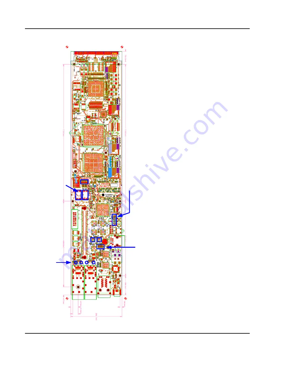
Figure 12: Location of LEDs and Displays (Top View) 

J1

4-F
P

G

A

 S

F

P


J1

5-D
S

P S
F

P


D21

U2
1

U2
2

2-C
h

ar

s

LE
D Di

sp
la

y

D22
D20
D16
D17

D3

D5

D6

D7

D1
5

D1
4

D1
3

D1
2

D1
9

D1
8

D1
1

D1
0

D9

D8

Summary of Contents for Tsi620

Page 1: ...Evaluation Board User Manual 60D7000_MA001_03 August 7 2009 6024 Silver Creek Valley Road San Jose California 95138 Telephone 408 284 8200 FAX 408 284 3572 Printed in U S A 2009 Integrated Device Tech...

Page 2: ...eserved or undefined are reserved for future definition IDT does not assume responsibility for conflicts or incompatibilities arising from the future definition of such items IDT products have not bee...

Page 3: ...tor 30 1 5 Configuration Options 31 1 5 1 DIP Switches 31 1 5 2 Jumpers 34 1 5 3 Push Button and Toggle Switch 34 1 6 Board Connectors 36 1 6 1 JTAG and FPGA Programming Connectors 36 1 6 2 Communicat...

Page 4: ...ed Device Technology www idt com 2 2 3 FPGA Hardware Load Facilities 49 2 2 4 Software Environment 50 2 3 DSP Software 51 2 3 1 Installing the DSP Software 51 2 3 2 Running the DSP Software 52 2 3 3 D...

Page 5: ...are can be used to test the board s PMC FPGA and DSP capabilities Terms AIF Antenna Interface AMC Advanced Mezzanine Card BB Baseband bps Bit per second BW Bandwidth Usually means row data including e...

Page 6: ...03 Formal August 2009 There are no technical changes to this document 60D7000_MA001_02 Formal November 2008 This version was updated to include information about the software on the Tsi620 evaluation...

Page 7: ...he following purposes To demonstrate the Tsi620 s potential application in a typical wireless baseband processing system To provide a hardware platform for customers to assess the Tsi620 s major featu...

Page 8: ...ub to provide high bandwidth data flow of the AMC backplane FPGA DSP and PrPMC module The processed data can be transmitted to the AMC sRIO backplane through the Tsi620 sRIO switch Both upstream and d...

Page 9: ...RJ45 connector Dual x1 sRIO ports to Tsi620 sRIO switch with 5 Gb bandwidth Altera Stratix3 FPGA EP3SL150 488 IOs 780 FBGA 29 x 29 mm 150K LE 9 4 Mb embedded RAM XGMII like Interface to sRIO switch w...

Page 10: ...ement networking connection 10M 100M Base T RJ45 to Stratix3 FPGA 1 2 2 5 Board Form Factor Single width full height and custom length AMC card 73 8W x 350L x 29H mm Supports a standard PrPMC module o...

Page 11: ...C MMC support Multiple voltage interface conversion 1 2 2 9 Power Management Meets AMC 0 specification for power management 12V power supply from AMC finger connector 12V 5A DC input connector for sta...

Page 12: ...3 125 Gbaud Conforms to AMC 1 and AMC 4 specification by PCIMG AMC 4 fabric port assignment support Type4 4x only Two 1x sRIO links between TCI6488 and Tsi620 XGMII interface to FPGA with 4x RapidIO p...

Page 13: ..._MODE_SEL 1 1 SP6 4x mode for FPGA I F SP_IO_SPEED 1 0 10 01 00 10 3 125 Gb Default 01 2 5 Gb 00 1 25 Gb S4 bit 4 3 SP_CLK_SEL 1 0 01 01 156 25 MHz SP n _PWRDN n 2 4 5 6 0 0 Port 2 4 5 6 are powered u...

Page 14: ...Bus Specification Revision 2 3 PCI Bus Power Management Specification Revision 1 1 IEEE1386 1 ANSI VITA 32 2003 PCI interface 32 bit bus 33 MHz 66 MHz 3 3V signal only Tsi620 internal PCI arbiter Tsi6...

Page 15: ...AT24C64B Supports I2C configuration loading Uses FT2233D USB to UART FIFO controller as USB to JTAG port converter Supports Tsi620 register access through JTAG port mini USB connector Table 2 PCI Int...

Page 16: ...lot shared with 12V power and local 3 3V Total power consumption including PrPMC and AMC slot should not be more than 60W Table 4 I2C Power Up Configuration Setting Pin Name Setting Description I2C_MA...

Page 17: ...tratix3 EP3SL150 in 780 pin BGA Package 29 x 29 mm 780 pin FBGA with 1 mm pitch Speed grade 3 Core voltage 1 1V Clock tree performance 450 MHz for 4 grade Maximum IO pins 480 Maximum allowed power con...

Page 18: ...3 2 3 RF Antenna Interface Compliant specifications CPRI specification v2 1 OBSAI v2 0 OBSAI RP3 v4 0 Supports 1x link to SFP connector with OBSAI 768 Mb or CPRI 614 4 Mb Supports 4x link to DSP with...

Page 19: ...link and JTAG emulation port see Figure 5 The TI TCI6488 is the major baseband processing engine on the Tsi620 evaluation board 1 3 3 1 TCI6488 DSP DSP core Triple C64X Core frequency 983 MHz 61 44Mx...

Page 20: ...ink 4x to FPGA with up to 768 Mbps per lane CPRI compatible 614 4 Mbps 1 2288 Gbps 2 4576 Gbps link rates OBSAI compatible 768 Mbps 1 536 Gbps 3 072 Gbps link rates DDR2 SDRAM 64Mx16b DQ 0 31 DQS p n...

Page 21: ...rt serial flash memory Serial flash can store the boot loader or software image Serial flash SF25L064 64 Mb 50 MHz SPI 3 3V device 3 3V to 1 8V level shifter is required between DSP and Serial flash 1...

Page 22: ...oller Functionality Board reset control Board power sequencing control and power monitoring Real time clock AMC MMC Memory management control Multi voltage level conversion UART port to USB interface...

Page 23: ...l reset controller to handle the reset control glue logic Reset Control Requirement Reset Control Logic System management controller Actel AFS256 FG256 Flash based mixed signal FPGA Supports multi vol...

Page 24: ...supported by IPMI firmware from uBlade The MMC design supports the basic requirements defined by the PICMIG AMC 0 and Intel IPMI v2 0 specifications For additional information about the MMC design con...

Page 25: ...DDR2 memory operation frequency run at slightly lower than their maximum specification Both DSP and DDR2 memory use the same clocking source at 61 44 MHz DSP core frequency is 983 MHz and DDR2 memory...

Page 26: ...6 Power Management 1 3 6 1 Power Supply and Consumption Analysis The board power distribution design must comply with AMC 1 power management requirements The AMC card has only single 12V supply availa...

Page 27: ...tracking which is used for silicon power sequencing control The LTM4604 4A 15 mm x 9 mm x 2 3 mm DC DC switching regulator generates 1 2V 1 5V 1 8V and 2 5v from either 5V rail or 3 3V rail 12V is im...

Page 28: ...functioning and waiting for 12V from the AMC backplane once the Hot Swap handler is closed 2 When 12V is powered up and SW2 is turned on the AFS600 signals to start 5V 1 5V and 1 2V 3 After 1 2V is p...

Page 29: ...TAG header AMC12Vin Plug DC12Vin 5A 5A DC DC SW LTM4601 5V 8A DC DC SW LTM4601 3 3V 12A DC DC SW LTM4601 1 1V_DSP 10A DC DC SW LTM4601 1 1V 10A DC DC SW LTM4604 DC DC SW LTM4604 DC DC SW LTM4604 1 8V...

Page 30: ...e Tsi620 is I2C master This bus includes the Tsi620 I2C EEPROM and two SFP optical transceivers 1 8V I2C bus The DSP is I2C master This bus includes the DSP I2C EEPROM and CDCL6010 Figure 10 Local I2C...

Page 31: ...s section describes the configuration options for the Tsi620 evaluation board 1 5 1 DIP Switches Switches S1 to S5 combine four small slide switches identified with numbers 1 to 4 see example in Figur...

Page 32: ...N 1 1 0 0 I2C Slave Boot ON ON OFF ON 0 0 1 0 EMAC Master Boot OFF ON OFF ON 1 0 1 0 EMAC Slave Boot ON OFF OFF ON 0 1 1 0 EMAC Forced Mode Boot ON OFF ON OFF 0 1 0 1 sRIO Boot 1 25 G CFG2 1 25 G Defa...

Page 33: ...ng Switch S4 Signal Assignment Default ON OFF Setting Bit 1 TSI620_SP_HOST 1 OFF ON Force PCI bus clock at 33 MHz OFF Set PCI bus clock at 66 MHz Bit 2 TSI620_I2C_DISABLE 1 OFF ON Set Tsi620_BCE to 0...

Page 34: ...SRESETN SW2 Toggle Switch POWER_ON OFF HotSwap_ OPEN CLOSE In non AMC Chassis mode after 12V applied SW2 functions as the power sequencing ON OFF switch In AMC Chassis mode SW2 functions as Hot Swap...

Page 35: ...4 J14 FPGA SFP J15 DSP SFP U35 Mini USB U26 FPGA RJ45 U34 GigE RJ45 SW2 ON OFF J4 Mictor U29 12Vin J2 DSP Emulator Port J10 Tsi620 JTAG P1 AMC Slot J5 FPGA Active Serial Programming U21 U22 2 Chars LE...

Page 36: ...d up IDT does not recommend re programming the Actel FPGA without consulting the IDT Technical Support team Tsi620 JTAG J10 A dedicated 16 pin header for the Tsi620 JTAG port this header is pin matche...

Page 37: ...SMA pair J7 J8 Connected to FPGA pin AE2 AF1a a LVDS or 2 5V Differential SMA pair J11 J12 Connected to FPGA pin AC2 AC1a MICTOR J13 30 72 MHz external clock sourceb b 3 3VTTL Connector Name Referenc...

Page 38: ...ual 60D7000_MA001_03 Intergrated Device Technology www idt com Figure 12 Location of LEDs and Displays Top View J14 FPGA SFP J15 DSP SFP D21 U21 U22 2 Chars LED Display D22 D20 D16 D17 D3 D5 D6 D7 D15...

Page 39: ...d D19 demonstrate rotated color display in the second interval They can be used as a board status indicator by the system controller which is implemented with the AFS600 FPGA Reference Designator Colo...

Page 40: ...J14 SFP optical transceiver transmitter is good D9 Orange J14 SFP optical transceiver receiver is good D10 Green J15 SFP optical transceiver transmitter is good D11 Orange J15 SFP optical transceiver...

Page 41: ...o User space applications The Linux kernel is based on version 2 6 26 available from www kernel org A few modifications have been done to the kernel to provide for better support of the EP8343 board a...

Page 42: ...sses the memory of an endpoint and displays its memory contents askdsp This communicates with a program executing on a DSP to perform a calculation Although both applications are relatively simple the...

Page 43: ...be run using a kernel and filesystem not stored on internal Flash memory A filesystem usable for this type of execution is provided on the CD however directions for configuring an NFS server is beyond...

Page 44: ...ng a new ramdisk set the name of the image file on the TFTP server by using the setenv ramdisk command for example setenv ramdisk ramdisk img Transfer the file and save it to flash using run install_r...

Page 45: ...y should be compiled using static libraries or appropriate shared libraries should be installed After modifications to the ramdisk are done unmount the filesystem gzip it and create a U Boot ramdisk i...

Page 46: ...S II 7 2 IDE or later Once the Altera software is installed create the directory which should contain all of the Alter FPGA loads and unpack the FPGA_loads zip file into this directory Next launch the...

Page 47: ...this app by typing create this app This command configures the makefile and other supporting files for the software application which the user has written The makefile will compile and link the users...

Page 48: ...ble as shown in the Altera USB Blaster Download Cable User Guide Before executing the FPGA software the FPGA hardware load must be programmed into the FPGA as follows 1 In the Tools pull down menu sel...

Page 49: ...rowse and then select the software project name srio_1250_x4 which matches the FPGA hardware load When the software project is selected the NIOS II ELF Executable text box is filled in with srio_test...

Page 50: ...s information about commands in the environment Typically the following command sequence is used 1 INIT To initialize the RapidIO masters and slaves 2 MNIT and MEM commands To initialize and display t...

Page 51: ...mmands GET and LOAD RMR and RMW RMSOAK INIT RESET MEM and MNIT The cmdRioDma c and cmdRioDma h files implement DMA related FPGA commands REMDEST REMRD REMWR REMSOAK 2 3 DSP Software The DSP software c...

Page 52: ...3 core DSP mounted on the Tsi620 evaluation board 3 Click Save and Quit and launch Code Composer Studio The CCStudio Parallel Debug Manager window appears with four entries ICEPICK_C_0 C6400PLUS_0 C64...

Page 53: ...st be started before the PMC software can be started 2 The FPGA INIT command must be executed before the PMC software can be started The correct Tsi620 configuration must be programmed into the EEPROM...

Page 54: ...54 Tsi620 Evaluation Board User Manual 60D7000_MA001_03 Intergrated Device Technology www idt com...

Page 55: ...09 CORPORATE HEADQUARTERS 6024 Silver Creek Valley Road San Jose CA 95138 for SALES 800 345 7015 or 408 284 8200 fax 408 284 2775 www idt com for Tech Support 408 360 1533 sRIO idt com Document 60D700...

Reviews: