S7-PRO Maintenance Manual (Basic Version V2.1)
INTERNAL
2012-07-20
Huawei Proprietary and Confidential
Copyright © Huawei Technologies Co., Ltd.
Page 42 of 97
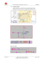
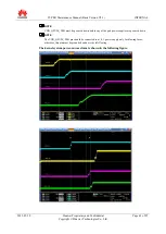
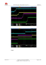
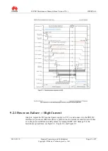
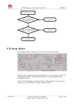
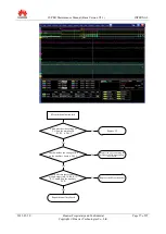
Mediapad power-on sequence:
Standard sequence:
VREG_S0A--->VREG_S1A--->VREG_S3A--->VREG_S2A--->VREG_L0A--->VREG_L21
A--->VREG_L7A--->VREG_L13A--->VREG_L16A--->VREG_L5A--->VREG_L6A--->VR
EG_S0B--->VREG_S3B--->VREG_L3B--->VREG_L11A--->--->TP_3V3--->VREG_L4B
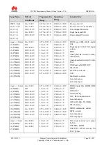
1. VDD_MEM (internal memory)
2. VDD_C1 (digital core circuits)
3. VDD_ISM1 and VDD_P3 (ISM 1.8 V power and most pad circuits/peripheral I/Os
respectively)
4. VDD_A3 (1.3 V RF, GPS ADC)
5. VDD_A2 (MIPI-DSI display)
6. VDD_A1, VDD_PXO, and VDD_MXO (PLLs, PXO, and MXO crystal power
respectively)
7. VDD_USBPHY_1P8 (1.8 V USB supply)
8. VDD_A5 (DACs and BBRx)
9. VDD_A4; VDD_A4_GPLL and VDD_A4_HFPLL (HDMI and MIPI-CSI; PLLs)
10. VDD_P2 (2.85 V SD card)
11. VDD_USBPHY_3P3 (3.3 V USB supply)
12. VDD_SC1 (1.1 V Scorpion core 1 – optional)
NOTE
1.
The core voltage (VDD_C1) needs to be powered up before the pad circuits
(VDD_PX) are powered up, so that internal circuits can take control of the I/Os and
pads.
2.
If pad voltages are powered up first, the output drivers may be stuck in unknown
states, and may cause high leakage current until VDD_C1 is powered on.
3.
The pad voltages must precede the analog voltages (VDD_AX), because the SSBIs
are initialized to the default state before VDD_AX is powered up (analog circuits are
controlled by SSBI).
4.
VDD_QDSP, VDD_SC1, and VDD_SC2 (QDSP and Scorpion core circuits) can be
powered up by the software after the MSM device has completed the boot process.
5.
Other non-critical supplies are included in the power-up sequence. Any other desired
supplies can be powered up by software after the sequence is completed.
6.
Each domain needs to reach the 90% value before the next domain starts ramping up.
For example, when VDD_C1 reaches 90% of the specified value, the VDD_P3 supply
can start ramping up.


