Rev. 1.71
102
April 11, 2017
Rev. 1.71
103
April 11, 2017
HT66F002/HT66F0025/HT66F003/HT66F004
Cost-Effective A/D Flash MCU with EEPROM
HT66F002/HT66F0025/HT66F003/HT66F004
Cost-Effective A/D Flash MCU with EEPROM
Although the A/D clock source is determined by the system clock f
SYS
, and by bits SACK2~SACK0,
there are some limitations on the maximum A/D clock source speed that can be selected. As the
recommended value of permissible A/D clock period, t
ADCK
, is from 0.5μs to 10μs, care must be
taken for system clock frequencies. For example, if the system clock operates at a frequency of
4MHz, the SACK2~SACK0 bits should not be set to 000B or 11xB. Doing so will give A/D clock
periods that are less than the minimum A/D clock period or greater than the maximum A/D clock
period which may result in inaccurate A/D conversion values.
Controlling the power on/off function of the A/D converter circuitry is implemented using the
ENADC bit in the SADC0 register. This bit must be set high to power on the A/D converter. When
the ENADC bit is set high to power on the A/D converter internal circuitry a certain delay, as
indicated in the timing diagram, must be allowed before an A/D conversion is initiated. Even if no
pins are selected for use as A/D inputs by configuring the corresponding pin-shared control bits, if
the ENADC bit is high then some power will still be consumed. In power conscious applications it
is therefore recommended that the ENADC is set low to reduce power consumption when the A/D
converter function is not being used.
The reference voltage supply to the A/D Converter can be supplied from either the internal ADC power
or from an external reference sources supplied on pin VREF or V
BG
voltage. The desired selection is
made using the SAVRS3~ SAVRS0 bits. As the VREF pin is pin-shared with other functions, when the
VREF pin is selected as the reference voltage supply pin, the VREF pin-shared function control bits
should be properly configured to disable other pin functions. When V
REF
or V
BG
is selected by ADC
input or ADC reference voltage, the OPA needs to be enabled by setting ENOPA=1.
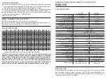
Reference
SAVRS[3:0]
Description
AV
DD
0000
ADC Reference Voltage comes from AV
DD
V
REF
0001
ADC Reference Voltage comes from External V
REF
V
REF
×2
0010
ADC Reference Voltage comes from External V
REF
×2
V
REF
×3
0011
ADC Reference Voltage comes from External V
REF
×3
V
REF
×4
0100
ADC Reference Voltage comes from External V
REF
×4
V
BG
×2
1010
ADC Reference Voltage comes from V
BG
×2
V
BG
×3
1011
ADC Reference Voltage comes from V
BG
×3
V
BG
×4
1100
ADC Reference Voltage comes from V
BG
×4
A/D Converter Reference Voltage Selection
A/D Converter Input Signal
All of the A/D analog input pins are pin-shared with the I/O pins on Port A and Port B as well as
other functions. The corredponding selection bits for each I/O pin in the PASR and PBSR registers,
determine whether the input pins are setup as A/D converter analog inputs or whether they have
other functions. If the pin-shared function control bits configure its corresponding pin as an A/D
analog channel input, the pin will be setup to be an A/D converter external channel input and the
original pin functions disabled. In this way, pins can be changed under program control to change
their function between A/D inputs and other functions. All pull-high resistors, which are setup
through register programming, will be automatically disconnected if the pins are setup as A/D
inputs. Note that it is not necessary to first setup the A/D pin as an input in the PAC and PBC port
control register to enable the A/D input as when the pin-shared function control bits enable an A/D
input, the status of the port control register will be overridden.
The A/D converter has its own reference voltage pin, VREF, however the reference voltage can
also be supplied from the power supply pin, a choice which is made through the SAVRS[
3
:0] in the
S
ADC2 register. The analog input values must not be allowed to exceed the value of V
REF.