


Rev. 1.20
61
October 28, 2020
BC45B4523
ADC_EN
ADC_Convert
TX_EN
ADC_Result
N/A
RX
FDDetectTime Operation
ADC-1
ADC-2
ADC-3
#1
IdleIRq
#2
RxIRq
ADC-4
ignored
detected
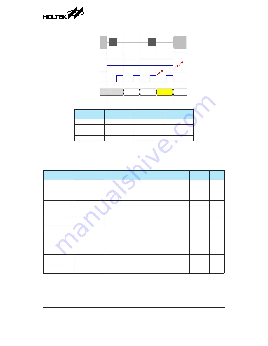
Field Detection Operation when FDDetectTime=“010”
FdDetectTime
[2:0]
Repeating
Times
FDDetectTime
[2:0]
Repeating
Times
000
1
100
16
001
2
101
32
010
4
110
64
011
8
111
128
FDDetectTime Configuration
Normally, the system offset may induce error to conversion result. ADCCalibrate command should be prior
executed to measure system offset and keep in internal buffer.
The registers associated with the RF amplitude detector are summarized in the following table.
Register
Address.Bit
Indication
Type
Default
Value
ADC_Rsln
Sector0-0x25.1
Configure ADC resolution which defines RF amplitude
input at RX pin
Read/Write
1
ADC_FastMode
Sector0-0x25.2
Define ADC mechanism and timing for conversion
Read/Write
0
ADC_FullScaleAdj Sector1-0x05.[1:0]
Define maximum input RF amplitude at pin RX for ADC
Read/Write
00
FD_MinLvl
Sector0-0x25.3
Define step size of ADC in Field Detection operation
Read/Write
0
ADC_Delay
Sector0-0x25.[5:4]
Define delay time for starting ADC conversion after all
related analog circuits are enabled
Read/Write
10
CDTxDelay
Sector0-0x31.2
Define wait time for RF amplitude settle, after
transmitter is enabled
Read/Write
1
CDAverage
Sector0-0x31.[1:0]
Define the number of average time in each
conversion in CardDetect Mode
Read/Write
00
FDAverage
Sector0-0x30.[1:0]
Define the number of average time in each
conversion in FieldDetect Mode
Read/Write
00
FDDetectTime
Sector0-0x30.[6:4]
Define the number of repetitive Field Detection
operation
Read/Write
100
ADC_Result_I
Sector0-0x26
ADC Conversion output, I-phase, which defines RF
amplitude at pin RX from FieldDetect and CardDetect Read Only
—
ADC_Result_Q
Sector0-0x27
ADC Conversion output, Q-phase, which defines RF
amplitude at pin RX from FieldDetect and CardDetect Read Only
—
Registers Associated with Field Detection and Card Detection