background image


AN-6130PCIe 


HOLT INTEGRATED CIRCUITS 


16 

PLX API’s 

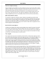
PLX API’s use a unique input parameter (BAR) to specify which LB memory space to read and write from. 

BAR stands for Base Address Register. BAR 0 and BAR 1 are reserved for the upstream PCIe.  BAR 2 and 

BAR 3 are used to provide separate memory spaces on the LB side. Bar 2 uses Space 0 and BAR 3 uses 

Space 1. The Space 0 and Space 1 PEX8311 registers are loaded with the desired starting BAR addresses 

at power up from the contents of the U6 EEPROM. Space 0 is reserved exclusively for the HI-6130 64KB 

memory space and is set to starting address 0x2000-0000. Space 1 is shared and modified on-the-fly in 

the API function calls to read/write to the output latches and reading the input status buffers. The 

latches are used to set the state of various inputs to the HI-6130 and the inputs are used to read HI-6130 

status and DIP switches. The Holt demo code includes several functions to read and write to the HI-6130 

memory space, latches and input status buffers. The API functions are located in HI6130.c. These 

functions use a PLX API to access the LB with either “PlxPci_PciBarSpaceRead(…)” or 

“PlxPci_PciBarSpaceWrite(…). One of the input parameters to these API’s is “bOffsetAsLocalAddr” this 

parameter controls how the API uses the U32 offset address. If “OffsetAsLocalAddr” is FALSE the input 

address is an offset address from the Space x value. If this parameter is TRUE the input address is the full 

address.  See the PLX API user’s manual for descriptions and usage of the API’s, BAR spaces and other 

input parameters associated with the PEX8311 and SDK API’s.


Device  

BAR 

Space 

Address 

Notes 

HI-6130 

0x2000-0000 

32K word range 

Output Latches 

0x2400-0000 

First location used 

Inputs 

0x2800-0000 

First location used 

Output Latches-2 

0x2C00-0000 

First location used 


The U6 EEPROM contains configuration data the PEX8311 uses to configure the LB at power up. The LB 
is configured for a 16-bit data bus, 14 wait states, Space0 and Space1 starting addresses/ranges, and 
disables the TA/Ready input. The PCI PLX sub-ID 3566 is also programmed into this EEPROM. This sub-ID 
is assigned by PLX exclusively for the Holt demo board.  

The PlxMon utility is launched from the Windows start menu or by double-clicking on the application 
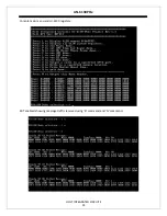
found in the /Plx/…/Bin folder. The PlxMon utility opening screen is shown below: 

Summary of Contents for AN-6130PCIe MIL-STD 1553

Page 1: ...16 PCI Express PCIe 1 1 slot on a PC running Windows 7 The HI 6130 is a single supply 3 3V rail BC MT RT1 RT2 Multi Terminal device for MIL STD 1553 dual redundant bus communications The card is bundl...

Page 2: ...documentation and software Topics Introduction Quick Start Guide Hardware Programming Reference Software Customization Summary Schematics and BOM Board Default Setup Set SW2 position 6 set to Off up p...

Page 3: ...ns 1 5 are user defined These may be used by the demo program in future releases Default DIP switch settings Metal brackets are provided for both full height and low profile PCIe cards Use the correct...

Page 4: ...in the HI 6130 The MSB bit 15 high indicates the HI 6130 READY is high which means the device is ready for the host to access the memory and registers in the device See the HI 6130 data sheet for more...

Page 5: ...ke it accessible to the scope probe If no external RT or test equipment is connected to the bus then use a 70 ohm termination resistor on the cable output or the signal will be distorted when viewed w...

Page 6: ...l Bus bridge and provides the interface between the PCIe slot and the local bus LB A CPLD translates the LB signals into CSn RDn and WRn strobe signals for the HI 6130 timings The CPLD also provides o...

Page 7: ...tion 4 PLX Debug Utilities Holt uses this utility to program the two EEPROMs The HI 6130 uses a 16 bit data bus 16 bit address bus and three more lines to select the device during reads and writes The...

Page 8: ...sions D1 ACKIRQ HI 6130 input D2 TP31 CPLD spare pin D3 RAMEDC HI 6130 Error detection correction input Set Low for this program D4 TXINHB HI 6130 Bus B inhibit input D5 TXINHA HI 6130 Bus A inhibit i...

Page 9: ...ved D6 IRQ 6130 HI 6130 interrupt output D7 N A Not defined D8 AUTOEN Set by the SW2 DIP switch 6 Input to HI 6130 for auto initialization from EEPROM D9 D5 Not used by connected to a pad on the PCB f...

Page 10: ...n signal is used by the CPLD to time when to de assert the CSn RWn or WRn signals to the HI 6130 and the internal latches and input buffers The ADSn signal from the LB is used by the CPLD to start the...

Page 11: ...AN 6130PCIe HOLT INTEGRATED CIRCUITS 11 CPLD Functional Block Diagram...

Page 12: ...R TRANSCEIVER POWER TEST MODE RT2SSF ACKIRQ RT1SSF MR RT2A4 0 AUTOEN RT2AP EECOPY BENDI RAMEDC RT1LOCK MTTCLK RT1A4 0 RT1AP MTSTOFF RT2LOCK RT1ENA RT2ENA BCENA MTENA Host Bus Interface HI 6130 Only IR...

Page 13: ...HI6130 c with accompanying header file HI6130 h To rebuild these projects the following three items are needed Holt demo projects contained on the CD ROM Microsoft Visual Studio 2012 Not Provided PLX...

Page 14: ...double click on the PCIe6130Test project file in the PCIe6130 test project folder 1 The Solution Explorer with the source files is shown on the left side If this is not seen then open the Solution Exp...

Page 15: ...led when the SDK is installed PLX PEX8311 RDK Hardware Reference Manual and the PLX PEX8311 data book Latest versions are available from the PLX website These are not included in the SDK Holt HI 6130...

Page 16: ...PLX API to access the LB with either PlxPci_PciBarSpaceRead or PlxPci_PciBarSpaceWrite One of the input parameters to these API s is bOffsetAsLocalAddr this parameter controls how the API uses the U32...

Page 17: ...RATED CIRCUITS 17 Select the Holt PCIe card from the Command menu or press the green icon button on the left and select the device with Dev ID 9056 and Ven ID 10B5 The PEX8311 consists internally of a...

Page 18: ...SIG obtained by becoming a PCI SIG member or a sub ID obtained from PLX For detailed information on these parameters and the PLX API s refer to the PLX SDK user s guide and data sheet on the PEX8311 F...

Page 19: ...s It s a good idea to review these two projects when first becoming familiar with the PLX API s These PLX projects do not run on the Holt PCIe card because the LB memory spaces are defined differently...

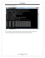
Page 20: ...ED CIRCUITS 20 The main menu will appear below Press D to display the HI 6130 system registers with labels followed by the same registers values formatted by beginning and end addressed rows followed...

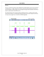
Page 21: ...ring the message To view the messages on a scope trigger on the rising edge of this signal with one probe and view the bus signal on another probe at the ABUS test point This waveform shows no RT resp...

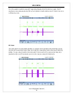
Page 22: ...ansmit occurs on a different bus stub RT1 Demo If an external RT is not immediately available on chip RT1 can be enabled in the HI 6130 by entering command B The waveform below shows the HI 6130 RT1 r...

Page 23: ...Codes using the Holt API library Optionally use the internal BC to transmit messages to the RT using the BC Major Minor frame demo N The bus connector should be terminated with 75 ohms or connected to...

Page 24: ...AN 6130PCIe HOLT INTEGRATED CIRCUITS 24 Console main menu and HI 6130 registers SRT enabled showing message traffic received using B command and N command...

Page 25: ...AN 6130PCIe HOLT INTEGRATED CIRCUITS 25 SRT showing Mode Codes received transmitted from an external BC...

Page 26: ...ffer 16 status input pins input ads ADS input input lwr LW R input input RT1MC8n RT2MC8n IRQn Interrupt inputs InOuts inout 15 0 DataBus 16 In out Data Bus pins Outputs output blast_q blast output out...

Page 27: ...01111 led5 Spare CS default add_L 8 b11111111 defaul all OFF endcase 16 bit 3 to 1 multiplexer always begin case add_L LatchAddress mux Latch First latches routed to mux InputsAddress mux InputBuffer...

Page 28: ...counter2 3 LEDWR 1 b1 turn off led else counter2 counter2 1 end Latched 16 GPIO s For Latch outputs always posedge WRn or negedge rstn begin if rstn Latch 16 b0001000000110000 Defaults LED1 On low TXI...

Page 29: ...assign DataBus oe mux 16 hZ Read the 16 inputs Misc Logic Interrupt MR assign nLINTi InputBuffer 4 InputBuffer 5 InputBuffer 6 Interrupt pins End of Misc The c_delay counter is used to slow down the...

Page 30: ...same hardware and software techniques would apply The devices that have a parallel interface would be the easiest to interface on the LB Some suggested ARINC 429 16 bit parallel parts are the HI 3582...

Page 31: ...the HI 6130 but does have some differences in the registers and pin outs The HI 6120 is simpler to use and cost less than the HI 6130 This change would require a revised board design not an add on bo...

Page 32: ...the same clock to generate the synchronized strobe signals internal to the CPLD and the CSn RDn and WRn strobe signals to the HI 6130 For a faster LB use up to 66MHz for the LB clock input of the PEX8...

Page 33: ...elopment Some guidance how to enhance and customize the design with additional MIL STD terminals ARINC 429 protocol IC s Discrete to Digital devices and memory was provided For questions regarding thi...

Page 34: ...CMX1200C3FTN245I 17 x 17 mm Address decoder Chip Selects RD WR Strobes 6130 RD WR Access LED indicators Status and DIP SW inputs Date Changes 9 19 2013 Rev A 12V 12V to 5V DC DC 3V3 HI 6130 PEX8311 Ti...

Page 35: ...0 B14 PETn0 B15 GND B16 PRSNT2 B17 GND B18 PRSNT1 A1 12V A2 12V A3 GND A4 JTAG2 A5 JTAG3 A6 JTAG4 A7 JTAG5 A8 3 3V A9 3 3V A10 PERST A11 GND A12 REFCLK A13 REFCLK A14 GND A15 PERp0 A16 PERn0 A17 GND A...

Page 36: ...61 0 01uF C73 0 01uF U7 LT1963AEST 2 5 VIN 1 GND 2 VOUT 3 RN11 742 08 3 103 J XX 1 2 3 4 5 6 7 8 C53 4 7uF 10V C50 0 1uF C74 0 1uF RN13 742 08 3 103 J XX 1 2 3 4 5 6 7 8 LED7 LED C62 0 1uF C71 0 01uF...

Page 37: ...E PT9A D8 PT9A PT7A PT9C E8 PT9B PT7B PT9D E9 PT6B PT7D PT10B CLK1 A9 PT6A PT7C PT10A A10 PT6C PT7E PT10C C9 PT6D PT7F PT10D C10 PT8C PT8A PT10E D9 PT8D PT8B PT10F D10 PT5C PT8C PT11A B9 PT5D PT8D PT1...

Page 38: ...0K 1 2 JP6 Solder Jumper TP13 C86 4 7uF 10V R64 330 1 2 R68 330 1 2 TP11 TP31 Sp L C97 10uF 16V LED8 LED C94 100nF C98 0 1uF pad 1 TP12 OSC2 50 0MHz OE 1 GD 2 OUT 3 VCC 4 LED11 LED C87 100nF C95 100nF...

Page 39: ...5 0 1uF 1 2 FB2 1 2 1 2 C110 01uF 1 2 C103 0 1uF 1 2 C113 4u7 10V 1 2 C106 0 1uF 1 2 C101 0 1uF 1 2 C107 0 1uF 1 2 C108 0 1uF 1 2 FB3 1 2 C112 0 1uF 1 2 VCCIO2 VCCIO3 Pin name sequence PR 640 1200 228...

Page 40: ...e Document Number Rev Date Sheet o f Doc PEX 8311 NC BALLS A 7 7 Tuesday August 13 2013 23351 Madero Mission Viejo CA 92691 www holtic com Holt Integrated Circuits U1B PEX83111 N C T1 N C P1 N C W6 N...

Page 41: ...Viejo CA 92691 A 1 1 www holtic com Title Size Document Number Rev Date Sheet o f NEW HI 6130 PCIe MIL STD 1553 Cable Holt Integrated Circuits 23351 Madero Mission Viejo CA 92691 A 1 1 www holtic com...

Page 42: ...1 Resistor 10K Ohm 5 1 10W 0603 R4 R5 R12 R21 R22 R26 R27 R39 R40 R43 R44 R 45 R46 R48 R49 R51 R57 R63 R65 R72 R133 P10KGCT ND Panasonic ERJ 3GEYJ103V 29 4 Header 1x3 Male 0 1 Pitch JP2 JP3 JP4 JP5 S1...

Page 43: ...EVISION HISTORY P N Rev Date Description of Change AN 6130PCIe NEW 09 27 2013 Release AN 6130PCIe A 06 30 2014 Revise for API demo program changes AN 6130PCIe B 03 04 2015 Update board photo on page 1...

Reviews: