background image

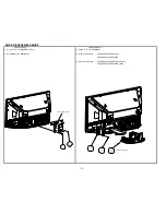
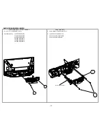
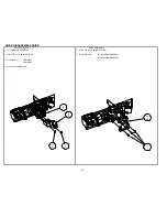
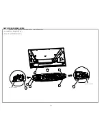
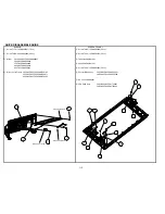
MIRROR COVER ASSY/SCREEN FRAME ASSY, LOW CABINET ASSY

   Screw M3M 4*14 P#MJ03663(2 Pcs.)

  Screw T1T 4*18 P#MJ03587(10 Pcs.)


PULL OUT THIS BAR

PULL OUT THIS BAR

QUICK DISASSEMBLE GUIDE

117

Summary of Contents for 50VF820 - 50" Rear Projection TV

Page 1: ...EFERENCE PARTS LIST IC UNIT 188 CAUTION These servicing instructions are for use by qualified service personnel only To reduce the risk of electric shock do not perform any servicing other than that contained in the operating instructions unless you are qualified to do so Before servicing this chassis it is important that the service technician read the IMPORTANT SAFETY INSTRUCTIONS in this servic...

Page 2: ...otective device built into the receiver by the manufacturer has become defective or inadvertently defeated during servicing Therefore the following checks should be performed for the con tinued protection of the customer and service technician Leakage Current Cold Check With the AC plug removed from the 120V AC 60Hz source place a jumper across the two plug prongs Using an insulation tester DC500V...

Page 3: ...it is not meant for the casual do it yourselfer Qualified technicians have the necessary test equipment and tools and have been trained to properly and safely repair complex prod ucts such as those covered by this manual Improperly per formed repairs can adversely affect the safety and reliability of the product and may void warranty Consumers should not risk trying to do the necessary repairs and...

Page 4: ...ally Sensitive ES Devices Some semiconductor solid state devices can be damaged easily by static electricity Such components commonly are called Electrostatically Sensitive ES Devices Examples of typical ES devices are integrated circuits and some field effect transistors and semiconductor chip components The following techniques should be used to help reduce the incidence of component damage caus...

Page 5: ...e standard technique as outlined in paragraphs 5 and 6 above Removal 1 Desolder and straighten each IC lead in one operation by gent ly prying up on the lead with the soldering iron tip as the solder melts 2 Draw away the melted solder with an anti static suction type sol der removal device or with solder braid before removing the IC Replacement 1 Carefully insert the replacement IC in the circuit...

Page 6: ...imp it around the IC pin Solder the IC connection 4 Route the jumper wire along the path of the cut away copper pattern and let it overlap the previously scraped end of the good copper pattern Solder the overlapped area and clip off any excess jumper wire At Other Connections Use the following technique to repair defective copper pattern at connections other than IC Pins This technique involves th...

Page 7: ...th a miniature alligator clip and apply heat to the pad area with a 30 watt iron until solder flows Do not apply heat for more than 3 seconds How to Replace Flat lC Required Tools Soldering iron iron wire or small awl De solder braids Magnifier 1 Remove the solder from all of the pins of a Flat lC by using a de solder braid 2 Put the iron wire under the pins of the Flat lC and pull it in the direc...

Page 8: ...ve previous solder as much as possible from the soldering point When soldering please perfectly melt the lead free solder to mix well with the previous solder 3 Soldering iron for lead free solder Melting point of lead free solder is higher than solder containing lead Use of a soldering tool with temperature control and with much thermal capacitance is recommended Recommended temperature control 3...

Page 9: ... Consult the dealer or an experienced radio television technician for help Modifications The FCC requires the user to be notified that any changes or modifications made to this device that are not expressly approved by Hitachi Home Electronics America Inc may void the user s warranty Cables Connections to this device must be made with shielded cables with metallic RFI EMI connector hoods to mainta...

Page 10: ... HDMI the HDMI logo and High Definition Multimedia Interface are trademarks or registered trademarks of HDMI Licensing LLC INPUTS Power Input AC 120V 60Hz Stand by Power Less than 1 Watt Power Consumption Refer to rear panel at the back of the T V Antenna input impedance 75 Ohm Channel coverage VHF Band 2 13 UHF Band 14 69 CATV Band 1 135 A I Video 1 0Vp p 75 Ohm S Video Luminance Y 1 0Vp p 75 Ohm...

Page 11: ...F820 2 2 2 1 1 1 1 1 2 1 1 5 50VG825 2 2 2 1 1 1 1 1 2 1 1 6 50VF820 2 2 2 1 1 1 1 1 2 1 1 7 8 9 10 REAR FRONT or SIDE No MODEL NAME POD Card IEEE 1394 A V In S video In Photo USB 1 60VG825 1 1 1 2 60VF820 1 1 1 1 3 55VG825 1 1 1 1 4 55VF820 1 1 1 1 5 50VG825 1 1 1 1 6 50VF820 1 1 1 1 7 8 9 10 Remark 1 Monitor out and Audio to HiFi share one terminal and switched by user menu See 5 9 Terminals and...

Page 12: ...84 H x 724 V 4 Panel size 0 7 5 Dot pitch 12 µm 6 Life time More than 20 000h Ta 25 C worst UV filter combination LCD panel is UV light sensitive device UV ray which illuminates LCD panel should be cut with three UV filters with 50 cut wavelength of 430nm 430nm 430nm nominal and 427nm 427nm 426nm worst combination 2 Lamp No Item Description 1 Input electricity 120W 120W 2 Manufacture Philips Panas...

Page 13: ...reen If so drapes or screens can be used to reduce the reflection or the TV can be located in a different section of the room If the TV s audio output will be connected to a Hi Fi system s external speakers the best audio performance will be obtained by placing the speakers equidistant from each side of the receiver cabinet and as close as possible to the height of the picture screen center For be...

Page 14: ... In jack Use this cable for the best sound quality IR Mouse Cable G LINK Cable ProvidedLC58E only Connect the IR Mouse to the IR Blaster output of your LCD Television when A V Network is used You must place the IR Mouse in front of the corresponding IR window of your cable box and VCR This connection allows your TV and the TV Guide On ScreenTM system to control your cable box and or VCR USB Cable ...

Page 15: ... for your desired sound level The volume level will be displayed on the TV screen These buttons also serve as the cursor left and right buttons when in MENU mode When the TV power is turned OFF at a volume level 31 or greater the volume level will default to 30 when the TV is turned ON However if it is set to a level 30 or less the volume level will be at the level it was set when the TV is turned...

Page 16: ...TER THE POWER ON NORMAL OPERATION BEGINNING OF COOL DOWN FOR 20 SEC TV CANíT ACCEPT ANY CODE IN THIS PERIOD EXCEPT BEGINNING S 5 SEC COOL DOWN FOR 6 MINUTES TV CAN ACCEPT REMOTE CONTROL AND FRONT BUTTONS LIGHT ON BLINKING LIGHT ON BLINKING INTERMEDIATE BLINKING 0 5 SEC CYCLE LIGHT ON SHORT BLINKING 0 3 SEC CYCLE LONG BLINKING 1 SEC CYCLE INDICATOR INDICATION MEANING ACTION LAMP LED TEMP LED POWER ...

Page 17: ...y insert connection cord plugs when connecting to side panel jacks If you do not the played back picture may be abnormal 2 If you have a S VHS VCR use the S INPUT cable in place of the standard video cable 3 If you have a mono VCR insert the audio cable into the left audio jack of your TV S VIDEO VIDEO AUDIO L MONO R INPUT 5 S VIDEO VIDEO AUDIO L MONO R INPUT 5 LC58 LC58E GENERAL INFORMATION 17 ...

Page 18: ...ugs when connecting to side panel jacks If you do not the played back picture may be abnormal 2 If you have a S VHS VCR use the S INPUT cable in place of the standard video cable 3 If you have a mono VCR insert the audio cable into the left audio jack of your TV S VIDEO VIDEO AUDIO L MONO R INPUT 5 S VIDEO VIDEO AUDIO L MONO R INPUT 5 Digital Camera Digital Camera USB USB Cable Cable PHOTO INPUT P...

Page 19: ... the Y PBPR jacks 6 INPUT 3 and INPUT 4 Y VIDEO can be used for composite video and component video input HDMI1 High Definition Multimedia Interface INPUT 1 ABOUT HDMI HDMI is the next generation all digital interface for consumer electronics HDMI enables the secure distribution of uncompressed high definition video and multi channel audio in a single cable Because digital television DTV signals r...

Page 20: ...bleCARD is installed wait until the second screen below appears The third screen below will appear if a channel is not authorized for viewing Press the EXIT button to exit the second screen Please take note of all information on the screen you will provide this information to your cable operator Call your cable operator and give them the information from the card to start your cable service Not an...

Page 21: ...ut You may use composite and component video signals for INPUT 3 and INPUT 4 It may be necessary to adjust TINT to obtain optimum picture quality when using the Y PBPR inputs To ensure no copyright infringement the MONITOR OUT output may be abnormal when using the Y PBPR jacks When using an HDMI input from a Set Top Box it is recommended that a 1080i or 720p input signal is used NOTE 1 Connect onl...

Page 22: ... product recycling and disposal information contact your local government agency or eRecycle org in California the Electronic Industries Alliance at www eiae org in the US or the Electronic Product Stewardship Canada at www epsc ca in Canada For more information call 1 800 HITACHI CAUTION A LAMP indicator will light when lamp becomes hot Unplug product s power cord from the AC outlet and allow lam...

Page 23: ...ord CAUTION The lamp is very hot and may cause fire or severe burns Wait at least 30 45 minutes to allow the lamp to cool before proceeding with lamp removal 2 Locate the Lamp Compartment on the left side of the LCD TV Lamp Compartment 120V Lamp Temp Power LC58 LC58E GENERAL INFORMATION 23 ...

Page 24: ...en removing the lamp unit to avoid injury to your fingers NOTE Do not put your hand in the Lamp Storage area after the Lamp Unit is removed your may get burned 5 Replace with the new lamp Place the removed lamp into the empty box of the replacement lamp Do not touch the front glass of the new lamp or its receptacle This may shorten the life of the lamp and reduce the picture quality Push the lamp ...

Page 25: ... main power switch NOTE This product contains lead and a lamp that contains mercury Dispose of this product and its lamp in accordance with applicable environmental laws For lamp recycling and disposal information go to www lamprecycle org For product recycling and disposal information contact your local government agency or eRecycle org in California the Electronic Industries Alliance at www eiae...

Page 26: ...hannel Push down on the wheel to access FAV Favorite Channel mode Favorite channel is only available for TV mode CURSOR PAD SELECT BUTTON TV DVD CBL STB PVR VCR The Cursor Pad is used as a cursor to navigate through the OSD and INPUT menu systems The Select button is used to Select Activate highlighted menu items VOLUME WHEEL TV AMP CD Scroll up and down to adjust the audio level of your TV Push d...

Page 27: ...s between DAY and NIGHT mode PIP BUTTON TV Press to show and change the Picture in Picture mode EXIT BUTTON TV CBL SAT Exits out of the OSD or INPUTS menu systems if their menu is displayed FAVORITE CHANNEL FAV CH button TV Press to enter access Favorite Channel FAV mode GUIDE BUTTON SAT STB CBL TV Accesses the channel guide of the TV or program guide of other devices INFO BUTTON TV CBL SAT Displa...

Page 28: ...ver all five video inputs have independent Aspect Style settings 2 Vertical position adjustments are directly available when you choose 4 3 EXPANDED ZOOM1 ZOOM2 or 16 9 ZOOM aspect style 4 3 STANDARD Use this aspect mode to display conventional 4 3 images Side panels gray areas are placed to the left and right of the image to preserve the original aspect ratio of the source Note Use this mode for ...

Page 29: ... Mode Sub Aspect 16 9 4 3 16 9 16 9 4 3 POP ANT Digital 16 9 Yes Yes Yes 480p 480i 16 9 Yes1 Yes1 ANT Analog 4 3 Yes Yes S Video Video PIP ANT Digital 16 9 Yes1 Yes 4 3 1080i 720p 16 9 Yes 480p 480i 16 9 Yes2 S Video Video PIP ANT Digital 16 9 Yes Yes2 16 9 1080i 720p 16 9 Yes 480p 480i 16 9 Yes2 S Video Video SPLIT ANT Digital 16 9 Yes Yes Yes 4 3 Yes Yes Yes 1080i 720p 16 9 Yes Yes 480p 480i 16 ...

Page 30: ... button to freeze three frames of the picture you are currently viewing only the 3 sub pictures will freeze Press the EXIT button to return to normal viewing This feature is useful for viewing a moving picture that has many details for example a close play in a sporting event or a golf swing NOTE 1 The default FREEZE mode is the MAIN freeze followed by the SPLIT freeze and then the STROBE freeze T...

Page 31: ...mp Holder Protection Operation Check 39 2 13 High Temperature Protection Operation Check 39 2 14 Temperature Sensor Data Setting 40 2 15 Checking of Temperature Sensor 41 2 16 Adjustment I2 C Parameter List 42 2 17 Adjustment OSD Flow Chart 79 2 18 Troubleshooting Flow Charts 88 IMPORTANT For many of the above adjustments it is necessary to have an HDTV 1080i or 720P signal generator SDTV 480P sig...

Page 32: ...DATA needs to be change press the keys to modify when finish press SELECT key to store the new DATA value normal condition C After finishing the necessary adjustment press the R C EXIT key or EXIT key on the side panel Adjustment mode is released and PTV set returns to normal condition 왗 왘 1 2 MEMORY INITIALIZE 1 2 1 MEMORY INITIALIZE OPER A TION NOTE The execution of this function returns the adj...

Page 33: ...n returns the adjustment made by the customer this will return all the adjustments to the original shipping conditions Procedure 1 Enter Adjustment mode by the method described in sub items 1 1 and 1 2 from item 1 Adjustment procedure start up 2 Get to the second page of Adjust Mode by pressing remote control Menu key once or with either the R C or front panel G H cursor keys several times 3 Selec...

Page 34: ...FSET value Adjustment range 2 5 GHOST ADJUSTMENT ADJUSTMENT PROCEDURE 1 ADJ SIGNAL Internal signal from IC Black window pattern with RGB raster signal ADJUSTMENT 2 RED GHOST LCD ADJUST MODE GHOST LCD ADJUST MODE GHOST R xx GHOST G xx GHOST B xx Press SELECT key test pattern will be displayed 1 Increase the I2C data by pressing cursor stick of handset until ghost appears at left side of the window ...

Page 35: ... 0 5 1 0 20mm 70 0 5 1 0 23mm H size marker 42 0 5 1 0 14mm 50 0 5 1 0 16mm 60 0 5 1 0 20mm 70 0 5 1 0 23mm 42 7mm 50 8mm 60 10mm 70 12mm Normal mode Outer edge of the circle Inner edge of the circle 5 3 3 5 Top and bottom of the circle is between outer edge and inner edge LC58 LC58E BACK TO ADJUSTMENTS 35 ...

Page 36: ...ance level is divided into 32 No 0_No 32 FOR EXAMPLE If customer require to change the white balance of 12th level of white to reddish increase the red value and adjust the white balance of 12th signal level see below I2C MENU LCDADJ GAMMA No 12 Adjustment STORE THE DATA TO TV SET LCD ADJ G C WRITE_press for several second After this procedure this new data will be write back to E2PROM It takes ab...

Page 37: ...NIFORMITY ADJUSTMENT PROCEDURE Adjustable luminance level is divided in 4 MIN 8 MIDL 20 MIDH 55 and HMAX 82 FOR EXAMPLE If a customer complains about the color uniformity at position 5 on the screen luminance level MIDH increase the BLUE or GREEN or RED value and adjust the color uniformity of position 5 I2C MENU LCDADJ C UNIF MIDH POINT No 5 STORE THE DATA TO TV SET LCD ADJ G C WRITE press for 2 ...

Page 38: ... GHOST B xxx Press SELECT key test pattern will be displayed Check that no ghost on right hand side of the window If there is decrease Ghost by pressing cursor stick of handset Press SELECT key of handset return to the LCD ADJUST MODE 3 Sub Ghost G adjustment Press key to select green Check and adjust sub ghost green with same procedure as Red SUB GHOST 4 Sub Ghost B adjustment Press key to select...

Page 39: ...flash red 3 Turn the set off and attach Lamp holder again 2 13 HIGH TEMPERATURE PROTECTION OPERATION CHECK Adjustment procedure 1 Remove EPF2 connector while the set is on 2 Check that the lamp is turned off and Temp indicator flash red 3 Turn the set off and attach EPF2 again 4 Remove EPF3 connector while the set is on 5 Check that the lamp is turned off and Temp indicator flash red 6 Turn the se...

Page 40: ...failed or not connected TEMP LED and LAMP LED are blinking alternately Cycle 1sec 2 14 2 Purpose It s important to set the limiting data correctly And it s better to use the automatic adjustment then human mistake is prevented Because each model needs the unique data that is different from another models 2 14 3 Adjustment Spec Adjustment procedure 1 Open ADJ menu and select Seine 2 Input the data ...

Page 41: ...d to be equal to data 71 alarm message OSD will be displayed in a minute Simplified method Check that front LEDs are not blinking alternately after power ON Device error blinking 2 15 1 Timing of the sensor operation as Appendix 3 minutes Device Error cannot be checked in this time 1 minute Average the data Start displaying OSD Power Device Error is checked once Starting of monitoring Starting of ...

Page 42: ...in EEPROM for Drive Micro Initial Data HEX Adjustment Mode OSD Adjustment Item Adjustment Range HEX LC58E LC58 LC57 Drive Up E7070 STRIPE_G0 LCD Adjust STRIPE0 G E7070 C4Bh 00 FF 008 STRIPE_G1 LCD Adjust STRIPE1 G E7070 C4Ch 00 FF 002 STRIPE_G2 LCD Adjust STRIPE2 G E7070 C4Dh 00 FF 000 STRIPE_G3 LCD Adjust STRIPE3 G E7070 C4Eh 00 FF 0FB STRIPE_G4 LCD Adjust STRIPE4 G E7070 C4Fh 00 FF 0FA STRIPE_B0...

Page 43: ...just G UNIF MIN 00 FF 1 B LCD Adjust B UNIF MIN 00 FF 1 No 1 25 LCD Adjust C UNIF NO 01 19 01 R LCD Adjust R UNIF MIN 00 FF 1 G LCD Adjust G UNIF MIN 00 FF 1 B LCD Adjust B UNIF MIN 00 FF 1 No 1 25 LCD Adjust C UNIF NO 01 19 01 R LCD Adjust R UNIF MIN 00 FF 1 G LCD Adjust G UNIF MIN 00 FF 1 B LCD Adjust B UNIF MIN 00 FF 1 G C_WRITE 2nd Page 2 2 Initial Data HEX Adjustment Mode OSD Adjustment Item ...

Page 44: ... 00 01 00 ID1_SLiCE_LEVEL ISLICEL ID1 Slice Level 00 03 00 ID1_AMP IRWIDON ID1 Amplitude Detect 00 01 01 ID1_PHASE_SEL IEDGES ID1 Phase Select 00 01 00 ID1_PHASE_WiDTH IRTIMS ID1 Detection Phase Width 00 01 00 3rd page 2 2 Initial Data HEX Adjustment Mode OSD Adjustment Item Adjustment Range HEX LC58E LC58 LC57 TC90103 G_READ_OUT GGSON Guide Slice Read Output 00 01 01 G_DETECT GGSJDG Guide Detecti...

Page 45: ...N B W Color Temperature B W 000 3FF 199 012 ISF Mode LCD DRIVE B SUB GAIN B W Color Temperature B W 000 3FF 148 013 LCD DRIVE VREF 00 FF 014 LCD DRIVE SHPR 00 0F 07 015 LCD DRIVE SHRG 00 0F 07 016 LCD DRIVE SHRB 00 0F 07 Drive Micro 2 2 Initial Data HEX Adjustment Mode OSD Adjustment Item Adjustment Range HEX LC58E LC58 LC57 Drive Micro E7070 017 LCD DRIVE NRSH LR 000 3FF 1F0 018 LCD DRIVE NRSH LG...

Page 46: ... HEX Adjustment Mode OSD Adjustment Item Adjustment Range HEX LC58E LC58 LC57 SEINE 036 Color Signal Round Coefficient for Noise Reduction NTSC 480i Input only 00 0D 0A 037 Color Signal Frame Difference Limit for Noise Reduction NTSC 480i Input only 00 1F 03 038 Enhance Movement Mode 00h Enhancer 2nd V filter OFF 01h Enhancer ON 02h 2nd V filter ON 03h Reserved 00 03 00 039 Enhancer Movement Mode ...

Page 47: ...nsor 1 Read Data 00 FF 075 Reserve Alarm 1 Start Temperature Setting 00 FF 4B 076 Reserve Alarm 1 Stop Temperature Setting 00 FF 41 FC6 1 20 Initial Data HEX Adjustment Mode OSD Adjustment Item Adjustment Range HEX LC58E LC58 LC57 FC6 001 ISF Mode Black Stretch 00h OFF 01h DBS 02h HBS 00 02 01 002 ISF Mode Black Correction 00h OFF 01h DBS 02h HBS 00 02 01 003 ISF Mode Histogram Gamma 00h OFF 01h A...

Page 48: ...e 3 Setting 000 3FF 0C0 033 ISF Mode Blue Line 4 Setting 000 3FF 100 034 ISF Mode Blue Line 5 Setting 000 3FF 140 035 ISF Mode Blue Line 6 Setting 000 3FF 180 FC6 3 20 Initial Data HEX Adjustment Mode OSD Adjustment Item Adjustment Range HEX LC58E LC58 LC57 FC6 036 ISF Mode Blue Line 8 Setting 000 3FF 200 037 ISF Mode Blue Line 10 Setting 000 3FF 280 038 ISF Mode Blue Line 12 Setting 000 7FF 300 0...

Page 49: ...0F 079 ISF Mode Y Vertical Enhancer OFF 00 01 00 FC6 5 20 Initial Data HEX Adjustment Mode OSD Adjustment Item Adjustment Range HEX LC58E LC58 LC57 FC6 080 ANT NTSC DAY 00 1F 0A 081 480i DAY 00 1F 0A 082 480p DAY 00 1F 0A 083 1080i 720p DAY 00 1F 0A 084 ISF Mode Y Vertical Enhancer Gain Adjustment ALL NIGHT 00 1F 0A 085 ANT 00 03 00 086 NTSC 00 03 00 087 480i 00 03 00 088 480p 00 03 00 089 ISF Mod...

Page 50: ...izontal Enhancer Clip OFF 1080i 720p 00 01 00 123 ANT 00 1F 3F 124 NTSC 00 1F 3F 125 480i 00 1F 3F 126 480p 00 1F 3F 127 ISF Mode Y Horizontal Clip Offset Level 1080i 720p 00 1F 3F FC6 7 20 Initial Data HEX Adjustment Mode OSD Adjustment Item Adjustment Range HEX LC58E LC58 LC57 FC6 128 ANT NTSC 480i 00 FF 00 129 ISF Mode Y Horizontal Non Linear Peaking 480p 1080i 720p 00 FF 00 130 ANT_Mode1 00 1F...

Page 51: ...F 14 170 Histogram Gamma APL Point 0 Gamma Select High 00 02 01 FC6 9 20 Initial Data HEX Adjustment Mode OSD Adjustment Item Adjustment Range HEX LC58E LC58 LC57 FC6 171 Histogram Gamma APL Point 1 Gamma Select High 00 02 00 172 Histogram Gamma APL Point 2 Gamma Select High 00 02 01 173 Histogram Gamma APL Point 3 Gamma Select High 00 02 02 174 Histogram Gamma APL Point 4 Gamma Select High 00 02 ...

Page 52: ... Bright Picture 000 3FF 8A 215 Gamma Line 9 Setting for Very Bright Picture 000 3FF 7C FC6 11 20 Initial Data HEX Adjustment Mode OSD Adjustment Item Adjustment Range HEX LC58E LC58 LC57 FC6 216 for Dark Picture 000 3FF 8E 217 for Standard 000 3FF 86 218 for Bright Picture 000 3FF 76 219 Gamma Line 8 Setting for Very Bright Picture 000 3FF 6C 220 for Dark Picture 000 3FF 7E 221 for Standard 000 3F...

Page 53: ...58 LC57 FC6 263 Black Stretch Black Correction Speed 00h Fast 10h Slow 00 10 00 264 Black Stretch Black Correction Reset APL 00 FF 0A 265 Black Stretch Black Correction Reset APL 00 FF 32 266 Black Stretch Black Correction Speed Up APL 00 FF 0E 267 Black Stretch Black Correction Speed Up Step 00h Direct 01h Slow FFh Fast 00 FF 00 268 Black Stretch Gain Up Step 0 00h Direct 01h Slow FFh Fastx8 00 F...

Page 54: ...n Contrast Correction Offset 00 FF 00 305 Black Correction Contrast Correction Value 00 FF FC6 15 20 Initial Data HEX Adjustment Mode OSD Adjustment Item Adjustment Range HEX LC58E LC58 LC57 FC6 306 Back Light Correction Speed 00h Fast 3Fh Slow 00 10 05 307 Back Light Correction Up Step 00h Direct 01h FFh Adjustment 4 256step 00 FF 40 308 Back Light Correction Down Step 00h Direct 01h FFh Adjustme...

Page 55: ...FC6 17 20 Initial Data HEX Adjustment Mode OSD Adjustment Item Adjustment Range HEX LC58E LC58 LC57 FC6 345 Shading OFF 10 00 FF 33 346 Shading 10 OFF 00 FF 1F 347 Shading 10 20 00 FF 3A 348 Shading 20 10 00 FF 26 349 Shading 20 30 00 FF 41 350 Shading 30 20 00 FF 2D 351 Histogram Detection Average Value 00 10 05 352 Histogram Area Start Position 00 07 04 353 Histogram Area End Position 00 07 07 3...

Page 56: ... 393 Maximum Brightness Level Detection 00 FF 394 Average Brightness Level Detection 00 FF 395 Brightness Histogram Detection 0 0000 FFFF 396 Brightness Histogram Detection 1 0000 FFFF 397 Brightness Histogram Detection 2 0000 FFFF 398 Brightness Histogram Detection 3 0000 FFFF 399 Brightness Histogram Detection 4 0000 FFFF 400 Brightness Histogram Detection 5 0000 FFFF 401 Brightness Histogram De...

Page 57: ... Adjustment Mode OSD Adjustment Item Adjustment Range HEX LC58E LC58 LC57 FC4 001 ISF Mode Dynamic Enhancer 00h APL Motion Adjustment Enhancer OFF 01h APL Synchronize Enhancer OFF 02h Motion Adjustment Enhancer 03h Active 00 03 03 002 ISF Mode Dynamic Contrast Correction 00h OFF 01h Active 00 01 01 003 Normal 00 FF 80 004 HDMI DVI Setup Cancel OFF 00 FF 80 005 ISF Mode Contrast Center DVI Setup Ca...

Page 58: ...0i 00 0F 00 032 720p 00 0F 00 033 ISF Mode Horizontal Enhance Coring Reserve 00 0F 00 FC4 3 19 Initial Data HEX Adjustment Mode OSD Adjustment Item Adjustment Range HEX LC58E LC58 LC57 FC4 034 ANT_Mode1 00 03 02 035 ANT_Mode2 5 00 03 02 036 NTSC 00 03 02 037 480i 00 03 02 038 480p 00 03 02 039 1080i 720p 00 03 01 040 ALL NIGHT 00 03 00 041 Reserve 00 03 01 042 ISF Mode Vertical Enhance Reserve 00 ...

Page 59: ... Off 00h CLIP ON 01h CLIP OFF 1080i 720p 00 01 00 FC4 5 19 Initial Data HEX Adjustment Mode OSD Adjustment Item Adjustment Range HEX LC58E LC58 LC57 FC4 074 ANT 00 0F 0B 075 NTSC 00 0F 0B 076 480i 00 0F 0B 077 480p 00 0F 0A 078 1080i 720p 00 0F 0A 079 ISF Mode Y Horizontal Enhancer Gain ALL NIGHT 00 0F 0A 080 ANT 00 0F 07 081 NTSC 00 0F 07 082 480i 00 0F 0F 083 480p 00 0F 0F 084 ISF Mode Y Horizon...

Page 60: ...07 116 ANT NTSC 480i 00 3F 00 117 ISF Mode Y Vertical Nonlinear Peaking 480p 1080i 720p 00 3F 00 FC4 7 19 Initial Data HEX Adjustment Mode OSD Adjustment Item Adjustment Range HEX LC58E LC58 LC57 FC4 118 ANT_Mode1 00 07 03 119 ANT Mode2 00 07 03 120 ANT Mode3 00 07 03 121 ANT Mode4 00 07 03 122 ANT Mode5 00 07 03 123 NTSC Composite 00 07 04 124 NTSC Y C 00 07 04 125 480i 00 07 04 126 480p 00 07 04...

Page 61: ... 1080i 00 FF 46 161 480i 00 1F 0D 162 APL Enhancer Correction Value 1080i 00 1F 0C 163 Horizontal Vertical Enhancer Setting Value 00 1F 164 Moving Enhancer Speed 00 10 0A FC4 9 19 Initial Data HEX Adjustment Mode OSD Adjustment Item Adjustment Range HEX LC58E LC58 LC57 FC4 165 ANT NTSC 480i 00 FF 12 166 Moving Enhancer Start Frame Differential 480p 1080i 720p 00 FF 0A 167 ANT NTSC 480i 00 FF 5A 16...

Page 62: ...2 480i 00 07 00 203 480p 00 07 00 204 Main Sub YNR Passage Level Limit 1080i 720p 00 07 00 FC4 11 19 Initial Data HEX Adjustment Mode OSD Adjustment Item Adjustment Range HEX LC58E LC58 LC57 FC4 205 ANT 00 07 04 206 NTSC 00 07 04 207 480i 00 07 04 208 480p 00 07 04 209 Main Sub YNR Input Level Gain 1080i 720p 00 07 04 210 Main YNR Reducing Gain 00 07 02 211 Sub YNR Reducing Gain 00 07 02 212 Main ...

Page 63: ...low 000 3FF 3FF 245 C M OFF Phase2 Hue Slope CCD Yellow 00h 128 80h 0 FFh 127 00 FF 80 FC4 13 19 Initial Data HEX Adjustment Mode OSD Adjustment Item Adjustment Range HEX LC58E LC58 LC57 FC4 246 C M OFF Phase3 Hue Center CCD Green Green Data Tint 360 1024 225 360 1024 640 280h 000 3FF 280 247 C M OFF Phase3 Hue Width CCD Green 000 3FF 100 248 C M OFF Phase3 Hue Clip CCD Green 000 3FF 3FF 249 C M O...

Page 64: ...ial Data HEX Adjustment Mode OSD Adjustment Item Adjustment Range HEX LC58E LC58 LC57 FC4 278 C M OFF Gain3 Hue Center CCD Green Green Data Tint 360 1024 225 360 1024 640 280h 000 3FF 280 279 C M OFF Gain3 Hue Width CCD Green 000 3FF 100 280 C M OFF Gain3 Hue Clip CCD Green 000 3FF 3FF 281 C M OFF Gain3 Hue Slope CCD Green 00h 128 80h 0 FFh 127 00 FF 80 282 C M OFF Gain4 Hue Center CCD Cyan Cyan D...

Page 65: ...per Green 000 3FF 3FF 313 C M OFF Phase3 Hue Slope Paper Green 00h 128 80h 0 FFh 127 00 FF 80 FC4 17 19 Initial Data HEX Adjustment Mode OSD Adjustment Item Adjustment Range HEX LC58E LC58 LC57 FC4 314 C M OFF Phase4 Hue Center Paper Cyan Cyan Data Tint 360 1024 293 2 360 1024 834 342h 000 3FF 342 315 C M OFF Phase4 Hue Width Paper Cyan 000 3FF 100 316 C M OFF Phase4 Hue Clip Paper Cyan 000 3FF 3F...

Page 66: ...ain5 Hue Slope Paper Blue 00h 128 80h 0 FFh 127 00 FF 80 FC4 19 19 Initial Data HEX Adjustment Mode OSD Adjustment Item Adjustment Range HEX LC58E LC58 LC57 FC4 346 C M OFF Gain6 Hue Center Paper Other_1 Data Tint 360 1024 000 3FF 000 347 C M OFF Gain6 Hue Width Paper Other_1 000 3FF 100 348 C M OFF Gain6 Hue Clip Paper Other_1 00 3FF 3FF 349 C M OFF Gain6 Hue Slope Paper Other_1 00h 128 80h 0 FFh...

Page 67: ...h 0 56 dB Y C 480i 00 0F 00 TC90103 2 12 Initial Data HEX Adjustment Mode OSD Adjustment Item Adjustment Range HEX LC58E LC58 LC57 TC90103 ANT NTSC 480i 016 ANT NTSC 00 03 01 017 Sharpness Noise Cancel Coring 00h 0 8 IRE 01h 1 6 IRE 02h 3 2 IER 03h 6 4 IRE Y C 480i 00 03 01 018 Noise Cancel Gain 00h OFF 01h 1 4 0h2 1 2 03h 1 00 03 00 019 LTI Gain LTI Luminance Transient Improvement 00h OFF 01h 1 8...

Page 68: ... 00 01 01 056 Vertical Y Noise Cancel Limiter 00h 8lsb 01h 16lsb 00 01 00 057 Vertical Y Noise Cancel Gain 00h 1 01h 2 00 01 00 TC90103 4 12 Initial Data HEX Adjustment Mode OSD Adjustment Item Adjustment Range HEX LC58E LC58 LC57 TC90103 ANT NTSC 480i 058 Vertical Y ON 00h OFF 01h ON 00 01 01 059 C NY Limiter 00h 16lsb 01h 24lsb 00 01 00 060 C NC Gain 00 01 00 061 C NC ON 00h OFF 01h ON 00 01 00 ...

Page 69: ...h 8 01h 16 02h 24 03h 32 00 03 01 094 1 Field Y Detection Slope Color Still Picture Edge 00h 1 2 03h 02 00 03 01 095 1 Field Y Detection Offset Color Still Picture Edge 00h Still Picture 0Fh Motion Picture 0C Center 00 0F 00 TC90103 6 12 Initial Data HEX Adjustment Mode OSD Adjustment Item Adjustment Range HEX LC58E LC58 LC57 TC90103 ANT NTSC 480i 096 Y Motion Picture Distinction Standard 00h 8 01...

Page 70: ...otion Picture 0Ch Center 00 0F 08 125 2 Field Detection 2nd Slope Threshold Y Still Picture Smooth 00h 0 01h 1 02h 2 03h 3 00 03 00 TC90103 8 12 Initial Data HEX Adjustment Mode OSD Adjustment Item Adjustment Range HEX LC58E LC58 LC57 TC90103 ANT NTSC 480i 126 2 Field Detection Slope Y Motion Picture Edge 00h 1 2 03h 02h Default 00 03 03 127 2 Field Detection Offset Y Motion Picture Edge 00h Still...

Page 71: ...h Still Picture 08h Default 00 0F 08 153 AGC Manual Setting AGC Auto Gain Control 00h OFF 01h ON 00 01 00 154 AGC Manual Gain Setting AGC Auto Gain Control 00 7F 28 155 AGC Sync Level Detection ON OFF AGC Auto Gain Control 00h OFF 01h ON 00 01 01 TC90103 10 12 Initial Data HEX Adjustment Mode OSD Adjustment Item Adjustment Range HEX LC58E LC58 LC57 TC90103 ANT NTSC 480i 156 AGC Peak Level Detectio...

Page 72: ... 00 0F 08 187 Memory Write Vertical Start Phase Adjustment 08h 8H 00h 0us 07h 7H 00 0F 08 188 Burst Gate Pulse Start Phase Adjustment 00h 0us 0Fh 4 44us 02h Default 3 58MHz unit 00 0F 02 TC90103 12 12 Initial Data HEX Adjustment Mode OSD Adjustment Item Adjustment Range HEX LC58E LC58 LC57 TC90103 ANT NTSC 480i 189 Clamp Pulse Horizontal Adjustment for Ghost Canceller Tuner 08h 1 185us 00h 0us 07h...

Page 73: ...Bit 000 3FF 002 Vertical Number High Bit 000 7FF 003 480i 00 03 02 004 480p 00 03 02 005 1080i 00 03 02 006 AFC loop gain control 00h H free running mode 01h gain low 02h gain middle 03h gain high 720p 00 03 02 007 480i 00 07 07 008 480p 00 07 07 009 1080i 00 07 07 010 Phase control Control for rough tune for HOUT 00h H sync center 01h center 3 125 02h center 6 25 03h center 9 375 04h 06h Leading ...

Page 74: ...ment Range HEX LC58E LC58 LC57 HDMI HDMI_1 2 001 VSYNC Clock detect Sync detect 1 00 07 002 HDCP Status 00 FF 003 Pixel clock 00 FF 004 N hardware value 1 Low 7 bit 00 FF 005 N hardware value 1 Middle 7 bit 00 FF 006 N hardware value 1 High 4 bit 00 FF 007 CTS hardware value 1 Low 7 bit 00 FF 008 CTS hardware value 1 Middle 7 bit 00 FF 009 CTS hardware value 1 High 4 bit 00 FF 010 ACR PLL hardware...

Page 75: ...CD DRIVE G SUB GAIN High 003 LCD DRIVE B SUB GAIN High 004 LCD DRIVE R SUB GAIN Medium 005 LCD DRIVE G SUB GAIN Medium 006 LCD DRIVE B SUB GAIN Medium 007 LCD DRIVE R SUB GAIN STD 008 LCD DRIVE G SUB GAIN STD 009 LCD DRIVE B SUB GAIN STD 010 LCD DRIVE R SUB GAIN B W 011 LCD DRIVE G SUB GAIN B W Drive Micro 012 LCD DRIVE B SUB GAIN B W 001 Black Stretch 002 Black Correction 003 Histogram Gamma 004 ...

Page 76: ...Dynamic Shoot Balance Coring Adjustment 480p 1080i 720p 093 ANT NTSC 480i 094 480p FC6 095 Y Vertical Enhancer Clip OFF 1080i 720p ISF Adjustment Mode Device OSD Item 096 ANT 097 NTSC 098 480i 099 480p 100 1080i 720p 101 ANT NTSC 480i NIGHT 102 480p NIGHT 103 Y Vertical Clip Offset Level 1080i 720p NIGHT 104 ANT NTSC 480i 105 Y Vertical Non Linear Peaking 480p 1080i 720p 106 Y Horizontal Enhancer ...

Page 77: ...NT Mode4 055 ANT Mode5 056 NTSC 057 480i 058 480p 059 1080i 060 720p 061 HDMI DVI 480i 062 HDMI DVI 480p VGA 063 HDMI DVI 1080i 064 HDMI DVI 720p 065 Reserve 066 Y Vertical and Horizontal Enhance Gain Reserve 067 ANT NTSC 068 480i 069 480p 070 Horizontal High Pass Filter Switch 1080i 720p 071 ANT NTSC 480i 072 480p 073 Y Horizontal Enhancer Clip Off 1080i 720p 074 ANT 075 NTSC 076 480i 077 480p 07...

Page 78: ...i 117 Y Vertical Nonlinear Peaking 480p 1080i 720p 118 ANT_Mode1 119 ANT Mode2 120 ANT Mode3 121 ANT Mode4 122 ANT Mode5 123 NTSC Composite 124 NTSC Y C 125 480i 126 480p 127 1080i 128 720p 129 HDMI DVI 480i 130 HDMI DVI 480p VGA 131 HDMI DVI 1080i 132 HDMI DVI 720p FC4 133 Y Coring Amplitude Reserve LC58 LC58E BACK TO ADJUSTMENTS 78 ...

Page 79: ... U D INPUT LCD ADJUST MODE RGB H POSITION V POSITION ENBW GHOST VCOM NRSH STRIPE S GHOST STREAK CH U D INPUT LCD ADJUST MODE RGB H POSITION V POSITION ENBW GHOST VCOM NRSH STRIPE S GHOST STREAK CH U D INPUT LCD ADJUST MODE RGB H POSITION V POSITION ENBW GHOST VCOM NRSH STRIPE S GHOST STREAK CH U D INPUT DATA Change DATA Change Same as left EXIT Select or OSD OFF ENBW Test Pattern Select Select DAT...

Page 80: ...PUT CH U D INPUT LCD ADJUST MODE RGB H POSITION V POSITION ENBW GHOST VCOM NRSH STRIPE S GHOST STREAK EXIT Select or DATA Change LCD ADJUST MODE STRIPE R0 STRIPE R1 STRIPE R2 STRIPE R3 STRIPE R4 OSD OFF STRIPE R0 Test Pattern Select Select DATA Change LCD ADJUST MODE STRIPE R0 STRIPE R1 STRIPE R2 STRIPE R3 STRIPE R4 OSD OFF STRIPE R4 Test Pattern Select Select x4 x4 LCD ADJUST MODE STRIPE G0 STRIP...

Page 81: ... LEVEL B SLOPE OSD OFF STRAK R Test Pattern Select Select DATA Change LCD ADJUST MODE R LEVEL R SLOPE G LEVLE G SLOPE B LEVEL B SLOPE OSD OFF STRAEK R Test Pattern Select Select LCD ADJUST MODE R LEVEL R SLOPE G LEVLE G SLOPE B LEVEL B SLOPE OSD OFF STRAEK B Test Pattern Select Select x4 x4 CH U D INPUT LCD ADJUST MODE GAMMA C UNIF MIN C UNIF MIDL C UNIF MIDH C UNIF MAX G C WRITE LCD DRIVE TEST PA...

Page 82: ...Select LCD ADJUST MODE POUNT No 0 R G B OSD OFF C UNIF MIN Test Pattern Select Select CH U D INPUT LCD ADJUST MODE GAMMA C UNIF MIN C UNIF MIDL C UNIF MIDH C UNIF MAX G C WRITE LCD DRIVE TEST PATTERN LPT FACT RESET EXIT Select or DATA Change LCD ADJUST MODE POINT No 1 R G B LCD ADJUST MODE GAM No 25 R G B x24 DATA Change LCD ADJUST MODE POINT No 1 R G B OSD OFF C UNIF MAX Test Pattern Select Selec...

Page 83: ... Software Version CH U D INPUT LCD ADJUST MODE GAMMA C UNIF MIN C UNIF MIDL C UNIF MIDH C UNIF MAX G C WRITE LCD DRIVE TEST PATTERN LPT FACT RESET EXIT Select or OSD OFF EXIT Select or OSD OFF Test Pattern CH U D INPUT LCD ADJUST MODE GAMMA C UNIF MIN C UNIF MIDL C UNIF MIDH C UNIF MAX G C WRITE LCD DRIVE TEST PATTERN LPT FACT RESET LCD ADJUST MODE GAMMA C UNIF MIN C UNIF MIDL C UNIF MIDH C UNIF M...

Page 84: ... SLICER M VBI SLICER S V CHIP CLOCK TEST MAINTENANCE MEMORY INIT OSD SELECT A CH U D INPUT LCD ADJUST MODE H TIMING V PHASE CCD READ OUT CCD SLICE CONT CCD SLICE LEVEL CCD SB DET CCD FIELD SEL DATA Change LCD ADJUST MODE ID1READ OUT ID1SLICE CONT ID1SLICE LEVEL ID1AMP ID1PHASE SEL ID1PHASE WIDTH LCD ADJUST MODE G READ OUT G DETECT G SLICE LEVEL CLOCK LINE READ DATA DATA ADD LINE 10 LINE 11 LINE 12...

Page 85: ...E TV GUIDE IR BLAST VBI SLICER M VBI SLICER S V CHIP CLOCK TEST 11 43 50 MAINTENANCE MEMORY INIT OSD SELECT A CH U D INPUT LCD ADJUST MODE TV GUIDE IR BLAST VBI SLICER M VBI SLICER S V CHIP CLOCK TEST MAINTENANCE MEMORY INIT OSD SELECT A A EXIT Select or EXIT Select or EXIT Select or CH U D INPUT LCD ADJUST MODE TV GUIDE IR BLAST VBI SLICER M VBI SLICER S V CHIP CLOCK TEST MAINTENANCE MEMORY INIT ...

Page 86: ...TA _ _ _ _ _ _ _ _ _ _ _ _ _ _ _ _ _ _ _ _ _ _ _ _ Select AD9880 and Press SELECT Press EXIT key CH U D INPUT LCD ADJUST MODE SEINE FC6 FC4 TC90103 AD9880 CXA2211 SiI9021 HDMI CH U D INPUT LCD ADJUST MODE AD9880 N0 DATA _ _ _ _ _ _ _ _ _ _ _ _ _ _ _ _ _ _ _ _ _ _ _ _ Select CXA2211 and Press SELECT Press EXIT key CH U D INPUT LCD ADJUST MODE SEINE FC6 FC4 TC90103 AD9880 CXA2211 SiI9021 HDMI CH U D...

Page 87: ... 0 2 2 3 2 3 2 LFE Timing Adjust 2 1 0 1 2 Back to Main EXIT Select or EXIT Select or EXIT Select or Maintenance Front End Display Video Format Display Audio Format Display System Check Display Out of Band Display CableCARD Display MMC Sniffer MMC Sniffer DATA Change System Check Software Version Main 01350001 1394 000003 1394NUID Contents Vender ID 000087 Chip ID 00001348CC Model ID 00000200 Vend...

Page 88: ...ange PiO01 D306 Red PiO00 1 Start 2 3 4 5 End LED OFF LIT After Program is loaded without error all LED will be turned off Any LED should not light If some errors occur LED will show the error pattern 1 Check that LED is not lit 2 If LED is lit refer to the following table and check the involved devices Location of LEDs front Signal Board LED1 D306 LED2 D305 LED3 D304 LED4 D303 LED5 D302 Digital M...

Page 89: ...Video Audio of Cable Air 5 Graphics All OSD 6 Flash Memory Loading Program 7 IEEE1394 Vivid Logic LC5X only IEEE1394 8 9 10 11 12 Video Decoder TC9010 CCD etc 13 14 Audio DSP AD9980 Audio cont SRS BBE 15 16 HDMI HDMI 17 A D Converter AD9980 Video 18 Sync Separator CXA2211 Sync 19 FC4 LC5X only Picture Cont 20 FC6 LC5X only Picture Cont LC58 LC58E BACK TO ADJUSTMENTS 89 2 18 TROUBLESHOOTING FLOW CH...

Page 90: ...Circuit No Role 21 RGB Processor TA1360 DP5X only Picture Cont VM 22 23 Drive u COM LC5X only LCD panel 24 Video SW Video 25 Audio SW Audio 26 Temp Sensor LC5X only Temperature sensor 27 28 29 30 31 32 LC58 LC58E BACK TO ADJUSTMENTS 90 2 18 TROUBLESHOOTING FLOW CHARTS ...

Page 91: ...Ensure Y signal at pin 9 of PHS2 OK NG Signal PWB defect RJ93 defect HJ01 defect Ensure Y signal at base of QJ10 QJ10 defect OK OK NG Ensure Y signal at pin 12 of IJ03 NG OK IJ03 defect RJ89 defect Ensure power at pin 20 and 19 of PHS2 OK NG Signal power PWB or Signal PWB defect Start HDMI 1 YES NO 1 LC58 LC58E 91 2 18 TROUBLESHOOTING FLOW CHARTS ...

Page 92: ... HJ04 Ensure Y signal at pin 4 of PHS2 OK NG Signal PWB defect RJP5 defect HJ04 defect Ensure Y signal at base of QJ22 QJ22 defect OK OK NG Ensure Y signal at pin 12 of IJ09 NG OK IJ09 defect RJP1 defect 1 LC58 LC58E BACK TO ADJUSTMENTS 92 2 18 TROUBLESHOOTING FLOW CHARTS ...

Page 93: ...ng components defect CJ55 RJ82 CJ60 RJ88 IJ05 defect Ensure audio signal at CJ50 and CJ57 Some of the following components defect RJ76 RJ78 RJ84 RJ85 IJ06 OK OK NG Ensure that digital signal at pin 1 2 3 and 16 of IJ05 OK NG Either RJ75 or RJ83 defect IJ03 defect Ensure power at pin 19 and 20 of PHS2 and pin 1 of PHS1 OK NG SIgnal PWB defect Start HDMI 1 YES NO 2 LC58 LC58E BACK TO ADJUSTMENTS 2 1...

Page 94: ...ollowing components defect CJE4 RJN3 CJE9 RJN9 IJ10 defect Ensure audio signal at CJC8 and CJE6 Some of the following components defect RJM6 RJM8 RJN5 RJN6 IJ11 OK OK NG Ensure that digital signal at pin 1 2 3 and 16 of IJ10 OK NG Either RJM5 or RJN4 defect IJ09 defect SIgnal PWB defect 2 LC58 LC58E BACK TO ADJUSTMENTS 94 2 18 TROUBLESHOOTING FLOW CHARTS ...

Page 95: ...RJ51 defect Ensure that SPDIF at pin 5 of IJ04 RJ56 defect OK OK NG Ensure that SPDIF at pin 29 of IJ03 OK NG IJ04 defect SIgnal PWB or Signal Power PWB defect Start IJ03 defect HDMI 1 YES NO Ensure that SPDIF at pin 1 and 2 RJK3 defect OK NG Ensure that SPDIF at pin 29 of IJ09 OK NG IJ04 defect IJ09 defect LC58 LC58E BACK TO ADJUSTMENTS 95 2 18 TROUBLESHOOTING FLOW CHARTS ...

Page 96: ...LC58 LC58E CIRCUIT BLOCK DIAGRAM TABLE OF CONTENTS 96 ...

Page 97: ...LC58 LC58E POWER SUPPLY BLOCK DIAGRAM TABLE OF CONTENTS 97 ...

Page 98: ...CONNECTION DIAGRAM TABLE OF CONTENTS LC58 LC58E 98 ...

Page 99: ...view PTW PFT3 Analog Tuner U301 PFT2 POWER PWB 0 0 0 0 240 325 240 IA02 PFH1 PPL PPDE FP01 I401 I501 PAN2 IA01 PSP1 Digital Main PWB Digital Sub PWB PINT IF03 IF02 IA04 PFA4 PFA3 PFA1 IF02 PSP2 CP01 ASSEMBLY DRAWINGS TABLE OF CONTENTS LC58 LC58E 99 ...

Page 100: ...106 I104 I103 IK02 PK01 IE02 I102 IF04 I101 IA10 JJ02 JJ03 IF01 PK02 PMV I202 I205 E104 E105 IE02 I501 IH03 I204 IH02 Rear view Digital Main PWB Side H I803 IG06 IJ02 I801 JUSB I105 I604 IC06 JJ01 PMS I206 IC04 I703 IG10 IK01 IC03 IC02 I203 I701 IK04 I606 IG05 IA05 I305 LC58 LC58E 100 ...

Page 101: ...BLY Rear view Digital Sub PWB Component Side XT01 PTS PSPI IV04 IT07 UT01 JT01 XT03 JIROUT HM01 JGLINK PSA IW02 IW03 IW11 IW12 IW05 Rear view Digital Sub PWB Pattern Side IW02 JS01 IT08 IW06 IW08 PMS IW09 IW10 LC58 LC58E 101 ...

Page 102: ... I902 D902 D952 T902 SW Transformer E942 SiG 5 6V PPT2 PPT3 D955 T901 SW Transformer D953 PPT1 I901 S903 Relay S902 Relay S901 Relay S904 Relay PPDE PA I905 OVP PROT I904 FB I906 FB D901 X901 Varistor LC5X POWER P W B I903 ACK F904 Temperature Limited Resistor LC58 LC58E 102 ...

Page 103: ...4 9 5 DRIVE P W B I7K0 Drive PWB Side A I7A0 I7F0 I750 I700 PDD P7A2 PDJ PSL PDE PDT PDP P7A0 P7K0 P7K0 Drive PWB Side B I601 LC58 LC58E 103 ...

Page 104: ...P W B LC58 LC58E PFF2B POWER INPUT EXIT CH VOL VOL CH MENU SELECT IR RECEIVER POWER LED LAMP LED TEMP LED PFF2A PFT1 S V L R PFT2 PFT3 IR RECEIVER LC58E ONLY LED PWB CONTROL PWB AV JACK PWB IR SUB PWB LC58 LC58E 104 ...

Page 105: ...LC58 chassis Model 50VF820 55VF820 60VF820 1 FRONT PANEL 2 REAR PANEL LC58 LC58E 105 ...

Page 106: ...LC58E chassis Model 50VG825 55VG825 60VG825 1 FRONT PANEL 2 REAR PANEL LC58 LC58E 106 ...

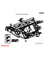
Page 107: ...TABLE OF CONTENTS FINAL WIRING DIAGRAM TABLE OF CONTENTS TABLE OF CONTENTS LC58 LC58E 107 Model 50VF820 60VF820 Model 50VG825 60VG825 ...

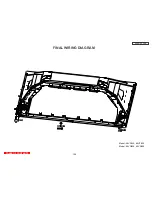
Page 108: ...TABLE OF CONTENTS FINAL WIRING DIAGRAM TABLE OF CONTENTS TABLE OF CONTENTS LC58 LC58E 108 Model 50VF820 60VF820 Model 50VG825 60VG825 ...

Page 109: ...TABLE OF CONTENTS TABLE OF CONTENTS TABLE OF CONTENTS FINAL WIRING DIAGRAM TABLE OF CONTENTS TABLE OF CONTENTS LC58 LC58E 109 Model 50VF820 60VF820 Model 50VG825 60VG825 ...

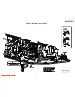
Page 110: ...TABLE OF CONTENTS FINAL WIRING DIAGRAM TABLE OF CONTENTS TABLE OF CONTENTS LC58 LC58E 110 Model 55VF820 Model 55VG825 ...

Page 111: ...TABLE OF CONTENTS TABLE OF CONTENTS TABLE OF CONTENTS FINAL WIRING DIAGRAM TABLE OF CONTENTS TABLE OF CONTENTS LC58 LC58E 111 Model 55VF820 Model 55VG825 ...

Page 112: ... P PH36031 60VG825 60VF820 P PH34961 Lower Rear Cover Assy 50VG825 50VF820 P PH34263 55VG825 55VF820 P PH36031 Lamp Assy P DP00675 60VG825 60VF820 P PH34961 LOOSE THESE SCREWS LOOSE THIS SCREW QUICK DISASSEMBLE GUIDE QUICK DISASSEMBLE GUIDE TABLE OF CONTENTS TABLE OF CONTENTS TABLE OF CONTENTS TABLE OF CONTENTS 112 ...

Page 113: ... Pcs Screw T1T 4 18 P MJ03587 Screw M3M 4 14 P MJ03663 Side AV Jack Assy 50 55 60VG825 P UE25301 50 55 60VF820 P UE25302 Main Chassis Assy 50 55 60VG825 P UE24551 LC58E 50 55 60VF820 P UE24552 LC58 BACK BONE METAL LIFT AND REMOVE 113 QUICK DISASSEMBLE GUIDE ...

Page 114: ...20 P NJ21512 60VG825 60VF820 P NJ21231 Lamp Power Unit P HA01234 Screw T1T 4 18 P MJ03587 DC Fan Assy DC Fan P GS01261 Holder P NJ22151 Exhaust Duct 50VG825 50VF820 P NJ09853 55VG825 55VF820 P NJ09853 60VG825 60VF820 Not applied Lamp Guide A 55VG825 55VF820 Only P NJ21531 Lamp Guide B 60VG825 60VF820 Only P NJ20281 Screw T1T 4 18 P MJ03587 LIFT AND REMOVE LAMP SOCKET METAL QUICK DISASSEMBLE GUIDE ...

Page 115: ...crew M3M 6 12 P MJ03621 4 Pcs Optical Block Assy 50VG825 P UE25271 Lamp Power Unit P HA01234 55VG825 P UE25272 Power Unit Holder P NT04861 60VG825 P UE25273 Power Unit Shield ME04472 50VF820 P UE25274 55VF820 P UE25275 60VF820 P UE25276 ENGINE BASE BRACKET QUICK DISASSEMBLE GUIDE 115 ...

Page 116: ... Screw M3M 3 8 P MJ03593 Screw T3E 3 12 P MJ03651 3 Pcs Screw T3E 3 12 P MJ03651 2 Pcs Drive PWB Assy 50 55 60VG825 P JP08481 50 55 60VF820 P JP08482 Exhaust Ducts P NJ09782 P NJ09793 Drive Shield P MD09382 QUICK DISASSEMBLE GUIDE 116 ...

Page 117: ...MIRROR COVER ASSY SCREEN FRAME ASSY LOW CABINET ASSY Screw M3M 4 14 P MJ03663 2 Pcs Screw T1T 4 18 P MJ03587 10 Pcs PULL OUT THIS BAR PULL OUT THIS BAR QUICK DISASSEMBLE GUIDE 117 ...

Page 118: ...E ASSY SPEAKER UNIT Screw T1T 4 18 P MJ03587 16 Pcs Screw T1T 4 18 P MJ03587 3 Pcs Screw T1T 4 18 P MJ03587 2 Pcs Speaker Unit P GM01671 MIRROR COVER ASSY SCREEN FRAME ASSY FIX METAL FIX METAL FIX METAL QUICK DISASSEMBLE GUIDE 118 ...

Page 119: ...VF820 P KS08438 Speakers P GK01391 60VG825 P KS08932 60VF820 P KS08435 Screw T2V 4 16 P MJ03442 2 Pcs Mirror Cover Frame 50VG825 50VF820 P QD38183 Control Block Assy 50 55 60VG825 P UE25281 55VG825 55VF820 P QD50671 50 55 60VF820 P UE25282 60VG825 60VF820 P QD38463 RC Lens P QX00921 LED PWB Assy 50 55 60VG825 P JT25001 50 55 60VF820 P JT25002 MIRROR RETAINER MIRROR RETAINER MIRROR RETAINER QUICK D...

Page 120: ...ssy 50VG825 50VF820 P KR03244 55VG825 55VF820 P KR03572 60VG825 60VF820 P KR03242 Screen Frame 50VG825 P QD51485 55VG825 P QD51486 60VG825 P QD51484 50VF820 P QD51482 55VF820 P QD51487 60VF820 P QD51481 CORNER METAL DUST COVER SCREEN FIX METALS QUICK DISASSEMBLE GUIDE 120 ...

Page 121: ... 2 Pcs Nut Washer P MK01431 2 Pcs Control PWB Assy 50 55 60VG825 P JT25001 Antena switch Box P HP00774 50 55 60VF820 P JT25002 Power Button P PC06541 Control Frame P PH37142 Screw T2V 4 12 P MJ03441 2 Pcs AV Jack PWB Assy 50 55 60VG825 P JT25001 50 55 60VF820 P JT25002 AV Jack Frame P PH34252 Screw T2B 4 12 P MJ03556 2 Pcs 50 55 60VG825 Only TERMINAL HOLDER QUICK DISASSEMBLE GUIDE 121 ...

Page 122: ...59 3 Pcs Power PWB Assy 50 55 60VG825 P JT24991 Digital Core Assy 50 55 60VG825 P UE24611 50 55 60VF820 P JT24992 50 55 60VF820 P UE24612 Screw T2B 3 12 P MJ03458 Signal PWB Assy 50 55 60VG825 P JT24981 50 55 60VF820 P JT24982 Power Cover P NA79181 SIGNAL PWB FRAME QUICK DISASSEMBLE GUIDE ...

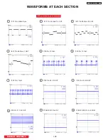
Page 123: ...Pin 54 Main PR OUT I401 Pin 55 Main PB OUT I401 Pin 56 Main Y OUT I700 Pin 12 Rin1 I700 Pin 10 Gin1 I700 Pin 7 Bin1 1 2 3 4 5 6 7 8 9 I700 Pin 24 VD OUT I700 Pin 25 HD OUT 11 P7A0 F0 K0 Pin 2 DY 10 I700 Pin 31 CLK OUT 12 P7A0 F0 K0 Pin 5 LCCOM Click on number to go to schematic 123 ...

Page 124: ...X P7A0 F0 K0 Pin 22 CLX P7A0 F0 K0 Pin 25 28 ENBX1 4 P7A0 F0 K0 Pin 29 NRG 13 14 15 16 17 18 19 20 21 P7A0 F0 K0 Pin 34 CLY I001 Pin 46 48 ALARM 0 2 23 I902 Pin 3 4 DL OUT 22 I901 Pin 7 8 STBY SWITCHED OUT 24 I902 Pin 1 DL OUT Click on number to go to schematic 124 IMPORTANT NOTE FOR HOT AREA USE AC CORD WITH FLOATING GROUND ...

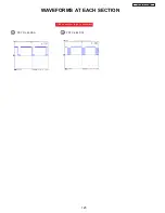
Page 125: ...LC58 LC58E WAVEFORMS AT EACH SECTION PST Pin 63 SDA PST Pin 64 SCL 25 26 Click on number to go to schematic 125 ...

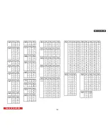
Page 126: ...tage 4 0 Symbol Pin No Voltage Pin No Voltage 24 3 4 54 0 84 0 114 0 PFA3 1 0 5 0 PPT2 1 5 7 11 0 25 0 55 0 85 0 115 0 2 10 1 6 0 2 0 0 12 0 26 0 1 56 4 5 86 0 116 0 3 0 7 0 3 0 0 13 0 27 0 57 4 5 87 0 117 0 4 NC 8 0 4 0 0 14 0 28 0 58 4 5 88 5 6 118 0 5 NC 5 0 15 0 29 0 59 0 89 5 6 119 0 Symbol Pin No Voltage 6 5 7 16 0 30 11 1 60 0 90 5 6 120 0 Symbol Pin No Voltage PTW 1 0 7 5 7 17 5 PFA4 1 0 2...

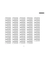
Page 127: ... 0 E 2 1 E 0 E 0 Symbol Pin No Voltage Symbol Pin No Voltage Symbol Pin No Voltage Symbol Pin No Voltage Symbol Pin No Voltage Q009 B 0 Q027 B 0 Q501 B 1 5 QA13 B 31 Q943 B 0 8 C 5 C 5 C 0 C 0 C 0 E 0 E 0 E 2 1 E 31 E 0 Symbol Pin No Voltage Symbol Pin No Voltage Symbol Pin No Voltage Symbol Pin No Voltage Symbol Pin No Voltage Q011 B 6 8 Q029 B 5 Q502 B 0 QA14 B 0 Q944 B 0 8 C 0 4 C 0 C 0 C 31 C ...

Page 128: ...02 1 0 5 3 3 4 9 2 0 2 0 6 3 3 5 10 Symbol Pin No Voltage Symbol Pin No Voltage Pin No Voltage 3 1 3 3 0 7 0 I903 1 27 3 I7A2 1 5 3 5 10 4 4 3 3 4 0 8 3 3 Symbol Pin No Voltage 2 29 4 2 5 3 6 10 4 5 5 I302 1 2 9 3 0 65 3 5 3 7 0 Symbol Pin No Voltage Pin No Voltage 2 0 4 5 3 4 0 8 15 6 Symbol Pin No Voltage U301 1 0 11 2 7 3 1 3 I591 1 0 2 5 12 3 8 4 5 Symbol Pin No Voltage Symbol Pin No Voltage P...

Page 129: ...gram the value of the parts is subject to be altered for improvement PRODUCT SAFETY NOTE Components marked with a and shaded have special characteristics important to safety Before replacing any of these components read carefully the PRODUCT SAFETY NOTICE of this Service Manual Don t degrade the safety of the receiver through improper servicing BASIC CIRCUIT DIAGRAM TABLE OF CONTENTS 129 ...

Page 130: ...ly the PRODUCT SAFETY NOTICE of this Service Manual Don t degrade the safety of the receiver through improper servicing BASIC CIRCUIT DIAGRAM All DC voltage to be measured with a tester 100k액 V Voltage taken on a complex color bar signal including a standard color bar signal Since this is a basic circuit diagram the value of the parts is subject to be altered for improvement 130 ...

Page 131: ...gram the value of the parts is subject to be altered for improvement PRODUCT SAFETY NOTE Components marked with a and shaded have special characteristics important to safety Before replacing any of these components read carefully the PRODUCT SAFETY NOTICE of this Service Manual Don t degrade the safety of the receiver through improper servicing BASIC CIRCUIT DIAGRAM TABLE OF CONTENTS 131 ...

Page 132: ...rcuit diagram the value of the parts is subject to be altered for improvement PRODUCT SAFETY NOTE Components marked with a and shaded have special characteristics important to safety Before replacing any of these components read carefully the PRODUCT SAFETY NOTICE of this Service Manual Don t degrade the safety of the receiver through improper servicing BASIC CIRCUIT DIAGRAM 132 ...

Page 133: ...rcuit diagram the value of the parts is subject to be altered for improvement PRODUCT SAFETY NOTE Components marked with a and shaded have special characteristics important to safety Before replacing any of these components read carefully the PRODUCT SAFETY NOTICE of this Service Manual Don t degrade the safety of the receiver through improper servicing BASIC CIRCUIT DIAGRAM 133 ...

Page 134: ...ly the PRODUCT SAFETY NOTICE of this Service Manual Don t degrade the safety of the receiver through improper servicing BASIC CIRCUIT DIAGRAM All DC voltage to be measured with a tester 100k액 V Voltage taken on a complex color bar signal including a standard color bar signal Since this is a basic circuit diagram the value of the parts is subject to be altered for improvement 134 ...

Page 135: ...rcuit diagram the value of the parts is subject to be altered for improvement PRODUCT SAFETY NOTE Components marked with a and shaded have special characteristics important to safety Before replacing any of these components read carefully the PRODUCT SAFETY NOTICE of this Service Manual Don t degrade the safety of the receiver through improper servicing BASIC CIRCUIT DIAGRAM 135 ...

Page 136: ...am the value of the parts is subject to be altered for improvement PRODUCT SAFETY NOTE Components marked with a and shaded have special characteristics important to safety Before replacing any of these components read carefully the PRODUCT SAFETY NOTICE of this Service Manual Don t degrade the safety of the receiver through improper servicing BASIC CIRCUIT DIAGRAM TABLE OF CONTENTS 1 136 21 ...

Page 137: ...ly the PRODUCT SAFETY NOTICE of this Service Manual Don t degrade the safety of the receiver through improper servicing BASIC CIRCUIT DIAGRAM All DC voltage to be measured with a tester 100k액 V Voltage taken on a complex color bar signal including a standard color bar signal Since this is a basic circuit diagram the value of the parts is subject to be altered for improvement 137 ...

Page 138: ...m the value of the parts is subject to be altered for improvement PRODUCT SAFETY NOTE Components marked with a and shaded have special characteristics important to safety Before replacing any of these components read carefully the PRODUCT SAFETY NOTICE of this Service Manual Don t degrade the safety of the receiver through improper servicing BASIC CIRCUIT DIAGRAM TABLE OF CONTENTS 138 2 3 4 ...

Page 139: ...it diagram the value of the parts is subject to be altered for improvement PRODUCT SAFETY NOTE Components marked with a and shaded have special characteristics important to safety Before replacing any of these components read carefully the PRODUCT SAFETY NOTICE of this Service Manual Don t degrade the safety of the receiver through improper servicing BASIC CIRCUIT DIAGRAM 139 26 25 ...

Page 140: ...rcuit diagram the value of the parts is subject to be altered for improvement PRODUCT SAFETY NOTE Components marked with a and shaded have special characteristics important to safety Before replacing any of these components read carefully the PRODUCT SAFETY NOTICE of this Service Manual Don t degrade the safety of the receiver through improper servicing BASIC CIRCUIT DIAGRAM 140 ...

Page 141: ...ly the PRODUCT SAFETY NOTICE of this Service Manual Don t degrade the safety of the receiver through improper servicing BASIC CIRCUIT DIAGRAM All DC voltage to be measured with a tester 100k액 V Voltage taken on a complex color bar signal including a standard color bar signal Since this is a basic circuit diagram the value of the parts is subject to be altered for improvement 141 ...

Page 142: ...c circuit diagram the value of the parts is subject to be altered for improvement PRODUCT SAFETY NOTE Components marked with a and shaded have special characteristics important to safety Before replacing any of these components read carefully the PRODUCT SAFETY NOTICE of this Service Manual Don t degrade the safety of the receiver through improper servicing BASIC CIRCUIT DIAGRAM ...

Page 143: ...he value of the parts is subject to be altered for improvement PRODUCT SAFETY NOTE Components marked with a and shaded have special characteristics important to safety Before replacing any of these components read carefully the PRODUCT SAFETY NOTICE of this Service Manual Don t degrade the safety of the receiver through improper servicing BASIC CIRCUIT DIAGRAM TABLE OF CONTENTS 143 5 6 7 8 9 10 ...

Page 144: ...CT SAFETY NOTICE of this Service Manual Don t degrade the safety of the receiver through improper servicing BASIC CIRCUIT DIAGRAM All DC voltage to be measured with a tester 100k액 V Voltage taken on a complex color bar signal including a standard color bar signal Since this is a basic circuit diagram the value of the parts is subject to be altered for improvement 144 11 12 13 16 17 18 19 20 ...

Page 145: ...CT SAFETY NOTICE of this Service Manual Don t degrade the safety of the receiver through improper servicing BASIC CIRCUIT DIAGRAM All DC voltage to be measured with a tester 100k액 V Voltage taken on a complex color bar signal including a standard color bar signal Since this is a basic circuit diagram the value of the parts is subject to be altered for improvement 145 11 12 14 16 17 18 19 20 ...

Page 146: ...m the value of the parts is subject to be altered for improvement PRODUCT SAFETY NOTE Components marked with a and shaded have special characteristics important to safety Before replacing any of these components read carefully the PRODUCT SAFETY NOTICE of this Service Manual Don t degrade the safety of the receiver through improper servicing BASIC CIRCUIT DIAGRAM 146 11 12 15 16 17 18 19 20 ...

Page 147: ...ly the PRODUCT SAFETY NOTICE of this Service Manual Don t degrade the safety of the receiver through improper servicing BASIC CIRCUIT DIAGRAM All DC voltage to be measured with a tester 100k액 V Voltage taken on a complex color bar signal including a standard color bar signal Since this is a basic circuit diagram the value of the parts is subject to be altered for improvement 147 ...

Page 148: ...e of the parts is subject to be altered for improvement PRODUCT SAFETY NOTE Components marked with a and shaded have special characteristics important to safety Before replacing any of these components read carefully the PRODUCT SAFETY NOTICE of this Service Manual Don t degrade the safety of the receiver through improper servicing BASIC CIRCUIT DIAGRAM TABLE OF CONTENTS TABLE OF CONTENTS 148 24 2...

Page 149: ...gram the value of the parts is subject to be altered for improvement PRODUCT SAFETY NOTE Components marked with a and shaded have special characteristics important to safety Before replacing any of these components read carefully the PRODUCT SAFETY NOTICE of this Service Manual Don t degrade the safety of the receiver through improper servicing BASIC CIRCUIT DIAGRAM TABLE OF CONTENTS 149 ...

Page 150: ...rcuit diagram the value of the parts is subject to be altered for improvement PRODUCT SAFETY NOTE Components marked with a and shaded have special characteristics important to safety Before replacing any of these components read carefully the PRODUCT SAFETY NOTICE of this Service Manual Don t degrade the safety of the receiver through improper servicing BASIC CIRCUIT DIAGRAM 150 ...

Page 151: ...gram the value of the parts is subject to be altered for improvement PRODUCT SAFETY NOTE Components marked with a and shaded have special characteristics important to safety Before replacing any of these components read carefully the PRODUCT SAFETY NOTICE of this Service Manual Don t degrade the safety of the receiver through improper servicing BASIC CIRCUIT DIAGRAM TABLE OF CONTENTS 151 ...

Page 152: ...4 IR03 C 4 IT04 A 1 DP01 C 2 IT05 A 1 DP02 C 2 IT06 A 1 DP03 C 2 IT07 A 1 DP20 C 2 IT09 A 2 DP21 C 2 IV03 B 4 DPS1 C 3 IV04 C 1 DPS2 C 3 IW01 B 3 DR01 C 4 IW02 A 3 DR02 C 4 IW03 A 3 DR03 C 4 IW05 B 3 DT01 B 1 IW11 A 3 IW12 A 3 IXJ1 C 1 IY01 B 3 XP01 C 3 IY02 B 3 XP05 C 2 IY03 B 3 XPS1 C 3 XT01 B 2 XT02 B 2 XT03 A 1 QP01 C 2 XT06 B 1 QP02 C 2 XT07 B 1 QP08 C 3 XY01 C 3 QR01 C 4 XY02 B 4 CRYSTAL FIL...

Page 153: ... A 3 QW02 B 2 IT13 B 4 QX01 C 2 IV01 B 1 QX02 C 2 IV02 B 1 QX03 C 2 IV05 B 2 QY01 C 2 IW04 A 3 QY02 C 2 IW06 A 3 IW07 B 3 IW08 B 2 IW09 B 2 XP04 A 2 IW10 B 2 XP06 C 3 IYJ2 B 2 XT04 A 4 XT05 B 4 XV01 B 1 XX05 C 4 QM01 C 4 XX06 C 4 QM02 C 3 XX07 C 3 CRYSTAL FILTER IC TRANSISTOR PRINTED CIRCUIT BOARDS SUBDIGITAL PWB Solder side BACK TO TABLE OF CONTENTS LC58 LC58E 1 2 3 4 A B C 153 ...

Page 154: ...QJ00 A 3 DF06 A 2 Q007 B 2 QJ01 A 3 DF07 A 3 Q008 B 2 QJ02 A 3 DF08 A 3 Q009 A 2 QJ03 A 3 DJ00 A 3 Q010 B 2 QJ04 A 3 DJ01 A 3 Q011 B 2 QJ05 C 3 DJ02 C 3 Q012 B 2 QJ06 A 3 DJ03 C 3 Q013 B 2 DJ04 A 4 Q014 B 2 DJ07 A 4 Q015 B 2 DJ08 A 3 Q016 B 2 D001 A 1 DJ09 A 3 Q017 B 2 D002 A 2 DJ10 A 4 Q018 A 2 D003 A 2 DJ11 A 4 Q021 B 2 D004 A 2 DJ12 A 4 Q022 A 1 D005 B 2 DJ13 C 3 Q023 A 1 D006 B 2 DJ14 A 3 Q024...

Page 155: ...SIGNAL PWB Solder side PRINTED CIRCUIT BOARDS BACK TO TABLE OF CONTENTS LC58 LC58E 155 ...

Page 156: ... C I602 B 2 I603 B 1 I606 B 2 I607 B 2 I700 A 4 I750 A 3 I7A0 C 1 I7A2 B 1 I7F0 A 2 I7K0 C 4 I7K1 B 4 I7K3 B 4 I7K4 B 4 I7K5 B 3 I800 A 1 I801 B 4 I802 B 4 I803 B 4 I804 A 1 I808 A 1 Q7F0 A 2 Q7F1 A 2 D610 A 1 X607 A 1 FILTER DIODE IC TRANSISTOR DRIVE PWB SEMICONDUCTOR LOCATION Component Side 156 ...

Page 157: ...B 1 Q7K3 B 1 Q7K4 B 2 D613 B 3 D7A0 A 2 D7A1 A 2 D801 B 1 D804 B 1 D805 A 4 D806 A 4 X604 B 4 X605 B 3 X606 A 4 X608 A 3 X609 A 3 X610 A 3 X611 A 3 X612 A 3 X613 A 3 X614 A 3 X615 A 3 X616 A 3 X617 A 3 X700 A 1 X702 A 1 X703 A 2 X704 A 2 X800 A 4 X801 A 4 X802 A 4 X803 A 4 X804 A 4 X805 A 4 IC CRYSTAL FILTER TRANSISTOR DIODE DRIVE PWB SEMICONDUCTOR LOCATION Solder Side 157 ...

Page 158: ...D943 A 4 I942 A 3 D944 A 3 D945 B 4 D946 B 4 D947 B 4 Q901 A 3 D948 B 4 Q942 A 3 D949 A 3 Q943 A 4 D950 C 4 Q944 B 4 D951 C 4 Q980 D 4 D952 A 3 Q981 D 4 D953 B 4 Q982 D 3 D954 C 4 D955 C 4 D958 C 4 D959 A 3 D901 B 2 D962 A 2 D902 B 1 D988 C 4 D903 A 1 D990 C 4 D904 B 3 D991 D 3 D906 B 2 D907 B 2 D909 B 2 D910 D 2 X901 D 1 D911 D 2 X902 D 1 D912 D 1 IC TRANSISTOR DIODE CRYSTAL FILTER POWER PWB SEMI...

Page 159: ...PRINTED CIRCUIT BOARDS POWER PWB Solder side BACK TO TABLE OF CONTENTS LC58 LC58E 159 ...

Page 160: ...PRINTED CIRCUIT BOARDS SENSOR PWB BACK TO TABLE OF CONTENTS LC58 LC58E Component side DL02 IC DIODE IL01 DL01 Component side Solder side 160 ...

Page 161: ...PRINTED CIRCUIT BOARDS AV JACK PWB Component side Solder side BACK TO TABLE OF CONTENTS LC58 LC58E Component side QM14 DM10 QM15 QM04 QM13 DIODE TRANSISTOR DM09 QM03 DM07 DM08 161 ...

Page 162: ...PRINTED CIRCUIT BOARDS DOOR SW A PWB Component side Solder side BACK TO TABLE OF CONTENTS LC58 LC58E 162 ...

Page 163: ...PRINTED CIRCUIT BOARDS DOOR SW B PWB Component side Solder side BACK TO TABLE OF CONTENTS LC58 LC58E 163 ...

Page 164: ...PRINTED CIRCUIT BOARDS FAN PWB Solder side BACK TO TABLE OF CONTENTS LC58 LC58E Component side Component side QM92 DIODE TRANSISTOR DM93 QM91 DM91 DM92 DM94 164 ...

Page 165: ...PRINTED CIRCUIT BOARDS IR SUB PWB BACK TO TABLE OF CONTENTS LC58 LC58E DM13 DM14 DM15 DM16 HM02 QM06 QM07 QM08 IC TRANSISTOR IM01 DIODE Component side Component side Solder side 165 ...

Page 166: ...01 DM02 DM03 DM04 DM05 DM11 DM12 DM18 DM19 HM01 QM01 QM05 QM10 QM11 QM12 TRANSISTOR DIODE PRINTED CIRCUIT BOARDS LED PWB BACK TO TABLE OF CONTENTS LC58 LC58E Component side Solder side Component side 166 ...

Page 167: ...PRINTED CIRCUIT BOARDS PJIG A PWB Solder side BACK TO TABLE OF CONTENTS LC58 LC58E Component side 167 ...

Page 168: ...PRINTED CIRCUIT BOARDS PJIG C PWB BACK TO TABLE OF CONTENTS LC58 LC58E Solder side Component side IJC1 IC 168 ...

Page 169: ...PRINTED CIRCUIT BOARDS TACT SW PWB BACK TO TABLE OF CONTENTS LC58 LC58E Component side Solder side 169 ...

Page 170: ...C 100000PF 16V TAPE 0 0 CP20 AA00937R CAP CHIP CERAMIC 10UF 10V 2012BK 0 0 CT11 AA01802R CCC103K50 B 16CT MCH18 0 0 CP21 0893179R CAP CHIP CERAMIC 100000PF 16V TAPE 0 0 CT12 AA00937R CAP CHIP CERAMIC 10UF 10V 2012BK 0 0 CP22 0893179R CAP CHIP CERAMIC 100000PF 16V TAPE 0 0 CT13 0893208R CAP 1608CHIP 1000PFKB 50V TAPE 0 0 CP23 AA00969R CAP CHIP2125 B 22UF6 3V 0 0 CT14 0893222R CAP 1608CHIP10000PFKB ...

Page 171: ...F6 3V 0 0 CT81 AA00968R CCC106M06 B 20CT 10UF 6 3V 2012M 0 0 CTJ5 0893122R CAP 1608CHIP 47PFJCH 50V TAPE 0 0 CT83 AA01231R 0 1UF 16V 1005 B CERAMIC CAPAC 0 0 CTJ6 0893123R CAP 1608CHIP 56PFJCH 50V TAPE 0 0 CT84 AA01231R 0 1UF 16V 1005 B CERAMIC CAPAC 0 0 CTJ7 0893222R CAP 1608CHIP10000PFKB 50V TAPE 0 0 CT85 0893113R CAP 1608CHIP 10PFCCH 50V TAPE 0 0 CTJ8 0893179R CAP CHIP CERAMIC 100000PF 16V TAPE...

Page 172: ... 0UF 16V 0 0 LT10 BA01234R HK2125 TYPE CHIP INDUCTOR 470N 0 0 CX03 0893179R CAP CHIP CERAMIC 100000PF 16V TAPE 0 0 LT11 BA01225R HK2125 TYPE CHIP INDUCTOR 100N 0 0 CX04 0893179R CAP CHIP CERAMIC 100000PF 16V TAPE 0 0 LT12 BA00191R COIL HCC39NJ16CT HK1608 0 0 CX05 0893179R CAP CHIP CERAMIC 100000PF 16V TAPE 0 0 LT14 BM10348R CHIP FERRITE BEAD BLM18PG121SN 0 0 CXJ1 AA01144R CERAMIC CAP 1608 B 1 0UF ...

Page 173: ...47R RES CHIP 1 16W 5 6K OHM 0 0 RT49 AQ00511R CHIP RESISTOR 10OHM 0 0 RPC1 0790001R CHIP RESISTOR RECJUMPER 1 16C16T1608 0 0 RT50 AQ00511R CHIP RESISTOR 10OHM 0 0 RPE1 0790001R CHIP RESISTOR RECJUMPER 1 16C16T1608 0 0 RT56 0790001R CHIP RESISTOR RECJUMPER 1 16C16T1608 0 0 RPG3 0790046R RES CHIP 1 16W 4 7K OHM 0 0 RT57 0790035R RES CHIP 1 16W 680 OHM 0 0 RPS1 0790037R RES CHIP 1 16W 1 0K OHM 0 0 RT...

Page 174: ...W48 0790051R RES CHIP 1 16W 10K OHM 0 0 CAPACITORS RW49 0790051R RES CHIP 1 16W 10K OHM 0 0 C004 AA01123R CCC105K10 B 16CT 0 0 RW50 0790051R RES CHIP 1 16W 10K OHM 0 0 C006 AA01123R CCC105K10 B 16CT 0 0 RW51 0790051R RES CHIP 1 16W 10K OHM 0 0 C007 0800326R CAP ELECTRO 100UF M 16V 0 0 RW52 0790051R RES CHIP 1 16W 10K OHM 0 0 C008 AA01141R CERAMIC CAPACITOR 0 1UF 16V 0 0 RW54 0790064R RES CHIP 1 16...

Page 175: ... CA50 0893208R CAP 1608CHIP 1000PFKB 50V TAPE 0 0 C410 0800352R CAP ELECTRO 470UF 10V 0 0 CA51 0893208R CAP 1608CHIP 1000PFKB 50V TAPE 0 0 C411 AA01123R CCC105K10 B 16CT 0 0 CA52 0800318R CAP ELECTRO 47UF M 25V 0 0 C412 AA01123R CCC105K10 B 16CT 0 0 CA53 0800318R CAP ELECTRO 47UF M 25V 0 0 C413 AA01141R CERAMIC CAPACITOR 0 1UF 16V 0 0 CA54 0800328R CAP ELECTRO 100UF M 35V 0 0 C414 AA01123R CCC105K...

Page 176: ... 0 0 D501 2348031M DIO MTZ J2 7ATA 0 0 KPD4 2784381M 0 60MM TAPED JUMP WIRE 0 0 D502 CC01921R SDS142WKF_PF 0 0 D503 CC01921R SDS142WKF_PF 0 0 COILS DA05 CC10521R DIODE 0 0 L002 BH00697R FILTER COIL 100UH 0 0 DA10 CC10521R DIODE 0 0 L003 BH00697R FILTER COIL 100UH 0 0 DA11 CC01921R SDS142WKF_PF 0 0 L005 BH00697R FILTER COIL 100UH 0 0 DA12 CC01921R SDS142WKF_PF 0 0 L006 BH00697R FILTER COIL 100UH 0 ...

Page 177: ...IP 1 16W 100 OHM 0 0 R121 0790024R RES CHIP 1 16W 100 OHM 0 0 RESISTORS R122 0790037R RES CHIP 1 16W 1 0K OHM 0 0 R001 0790001R CHIP RESISTOR RECJUMPER 1 16C16T1608 0 R123 0790037R RES CHIP 1 16W 1 0K OHM 0 0 R002 0790024R RES CHIP 1 16W 100 OHM 0 0 R124 0790037R RES CHIP 1 16W 1 0K OHM 0 0 R004 0790001R CHIP RESISTOR RECJUMPER 1 16C16T1608 0 R125 0790037R RES CHIP 1 16W 1 0K OHM 0 0 R006 0790046R...

Page 178: ...UMPER 1 16C16T1608 0 0 R485 0790034R RES CHIP 1 16W 560 OHM 0 0 R324 0790001R CHIP RESISTOR RECJUMPER 1 16C16T1608 0 0 R486 0790034R RES CHIP 1 16W 560 OHM 0 0 R325 0195250R RES 2125 CHIP JAMPER WIRE 0 0 R487 0790034R RES CHIP 1 16W 560 OHM 0 0 R401 AQ00164R CHIP RESISTOR 1 16W 75OHM TAPE 0 0 R500 0790064R RES CHIP 1 16W 100K OHM 0 0 R402 AQ00164R CHIP RESISTOR 1 16W 75OHM TAPE 0 0 R501 0790064R R...

Page 179: ...K OHM TAPE 0 0 RA32 AQ00194R RES CHIP 1 16W 1 0K OHM TAPE 0 0 RF21 0790001R CHIP RESISTOR RECJUMPER 1 16C16T1608 0 0 RA33 0790058R RES CHIP 1 16W 39K OHM 0 0 RF22 0790001R CHIP RESISTOR RECJUMPER 1 16C16T1608 0 0 RA34 0790052R RES CHIP 1 16W 12K OHM 0 0 RF23 0790037R RES CHIP 1 16W 1 0K OHM 0 0 RA35 0790024R RES CHIP 1 16W 100 OHM 0 0 RF24 AQ00196R RES CHIP 1 16W 1 2K OHM TAPE 0 0 RA36 0790037R RE...

Page 180: ... ED00383 PLUG 4P JST2 5ROCK 0 C959 0243503R CAP CERAMIC 150PF K B 500V 0 0 PINT 2902261 PLUG PIN SUB MINI 2P 0 0 C980 0880194R CAP POLYESTER 0 1UF J 50V 0 0 PPDE ED02813 4P VH CONNECTOR PLUG 2 4 NC 0 0 C981 0800319R CAP ELECTRO 47UF M 35V 0 0 PPL 2674281 3P B PLUG PIN 0 0 C982 0880194R CAP POLYESTER 0 1UF J 50V 0 0 PPT1 ED03203 6P 2 5MM PITCH CONNECTOR TAC L06X A3 0 0 PPT2 ED04332U 2 54MM PITCH 20...

Page 181: ...3 0700041M RES CARBON FLM 1 16W 1 0K JB 0 0 K019 2784381M 0 60MM TAPED JUMP WIRE 0 0 R924 AT04428M ASR 12 TB 390KOHM J 0 0 K020 2784381M 0 60MM TAPED JUMP WIRE 0 0 R925 0700057M RES CARBON FLM 1 16W 18K JB 0 0 K021 2784381M 0 60MM TAPED JUMP WIRE 0 0 R926 0700054M RES CARBON FLM 1 16W 10K JB 0 0 K022 2784381M 0 60MM TAPED JUMP WIRE 0 0 R927 0700054M RES CARBON FLM 1 16W 10K JB 0 0 K023 2784381M 0 ...

Page 182: ...UF 16V 0 0 C7F5 AA01347R CERAMIC CAPACITOR 0 1UF 25V B 0 0 C615 AA00968R CCC106M06 B 20CT 10UF 6 3V 2012M 0 0 C7F7 0893208R CAP 1608CHIP 1000PFKB 50V TAPE 0 0 C617 AA00968R CCC106M06 B 20CT 10UF 6 3V 2012M 0 0 C7F8 AA01347R CERAMIC CAPACITOR 0 1UF 25V B 0 0 C618 0893232R CAP 1608CHIP 100000PFZF25V TAPE 0 0 C7F9 AA01141R CERAMIC CAPACITOR 0 1UF 16V 0 0 C619 AA01141R CERAMIC CAPACITOR 0 1UF 16V 0 0 ...

Page 183: ...0 0 R653 0790024R RES CHIP 1 16W 100 OHM 0 0 I750 CK38931U IC L3E07070K0A 0 0 R656 0790024R RES CHIP 1 16W 100 OHM 0 0 I7A0 CK39631U IC L3E06110D0A 0 0 R665 0790001R CHIP RESISTOR RECJUMPER 1 16C16T1608 0 0 I7A2 CK06371R ANALOG MONOLITHIC IC BA4560F 0 0 R666 0790001R CHIP RESISTOR RECJUMPER 1 16C16T1608 0 0 I7F0 CK39631U IC L3E06110D0A 0 0 R667 0790001R CHIP RESISTOR RECJUMPER 1 16C16T1608 0 0 I7K...

Page 184: ...M 0 0 R7L8 0790001R CHIP RESISTOR RECJUMPER 1 16C16T1608 0 0 R755 0790064R RES CHIP 1 16W 100K OHM 0 0 R7L9 0790001R CHIP RESISTOR RECJUMPER 1 16C16T1608 0 0 R756 0790064R RES CHIP 1 16W 100K OHM 0 0 R7M3 0790054R RES CHIP 1 16W 18K OHM 0 0 R757 0790064R RES CHIP 1 16W 100K OHM 0 0 R7M5 0790024R RES CHIP 1 16W 100 OHM 0 0 R758 0790024R RES CHIP 1 16W 100 OHM 0 0 R7M7 0790047R RES CHIP 1 16W 5 6K O...

Page 185: ...E00412R 3218 CHIP LC FILTER 0 0 KM05 2784381M 0 60MM TAPED JUMP WIRE 0 0 KM07 2784381M 0 60MM TAPED JUMP WIRE 0 0 CONNECTORS JACKS KM10 2784381M 0 60MM TAPED JUMP WIRE 0 P7A0 EA02263R PLUG 54104 3631 0 0 KM37 2784381M 0 60MM TAPED JUMP WIRE 0 P7A2 EA02134R 5P SMT PH CONNE POST LF 0 0 KM38 2784381M 0 60MM TAPED JUMP WIRE 0 P7F0 EA02263R PLUG 54104 3631 0 0 KM39 2784381M 0 60MM TAPED JUMP WIRE 0 P7K...

Page 186: ...RM48 0700032M RES CARBON FLM 1 16W 220 JB 0 RL03 0790024R RES CHIP 1 16W 100 OHM 0 0 RM49 0700041M RES CARBON FLM 1 16W 1 0K JB 0 RL04 0790051R RES CHIP 1 16W 10K OHM 0 0 RM50 0100065M RES CARBON FLM 1 8W 1K JB 0 RL05 0790001R CHIP RESISTOR RECJUMPER 1 16C16T1608 0 0 RM52 0700032M RES CARBON FLM 1 16W 220 JB 0 RL06 0790001R CHIP RESISTOR RECJUMPER 1 16C16T1608 0 0 RM53 0700046M RES CARBON FLM 1 16...

Page 187: ...MM 0 0 ESP1 EF22806 8P XA SM CONNECTOR 1800 500MM 0 0 ESP2 EF24761 7P XAP 5P SMR CONNECTOR 600MM 0 0 ETEM1 2908704 4J PH CONNECTOR 750MM 0 0 ETW EF23314 5P PH PH CONNECTOR 1250MM 3NC 0 0 EUSB EW08451 4J USB CABLE L 1 0 0 ESPL EF24871 5J SMP FASTON CONNECTOR 750 60 0 0 ESPR EF24881 4J SM FASTON CONNECTOR 750 600 0 0 EFF2 EF03315S 5J XA CONNECTOR 120MM 0 0 EFT EF20973 13P XA CONNECTOR 220MM 0 0 MISC...

Page 188: ...W02 CK08271R DIGITAL MONOLITHIC IC SN74LVC244PW OCTAL BUFFER DRIVER WITH 3 STATE OUTPUTS FOR POD IF SUBDIGITAL 0 0 33 IW03 CK08271R DIGITAL MONOLITHIC IC SN74LVC244PW OCTAL BUFFER DRIVER WITH 3 STATE OUTPUTS FOR POD IF SUBDIGITAL 0 0 34 IW04 CK38327R DIGITAL MONOLITHIC IC SN74LVC1G86DCKR SINGLE 2 INPUT EXCLUSIVE OR GATE SUBDIGITAL 0 0 35 IW05 CK51161R PI5C32X245BEX 16 BIT 2 PORT BUS SWITCH SUBDIGI...

Page 189: ...AMP DRIVE 0 0 82 I7K3 CK18641R IC BA10358F E2 T1 DUAL GROUND SENSE OP AMP DRIVE 0 0 83 I800 CK38379R ANALOG MONO SI 3010KM TL 1 A LOW DROPOUT VOLTAGE REGULATOR DRIVE 0 0 84 I801 CK38379R ANALOG MONO SI 3010KM TL 1 A LOW DROPOUT VOLTAGE REGULATOR DRIVE 0 0 85 I802 CK38372R DIGITAL MONO IC SI 3018KM LOW DROPOUT 1 8 V VOLTAGE REGULATOR DRIVE 0 0 86 I803 CK38375R DIGITAL MONO IC SI 3033KM LOW DROPOUT ...

Page 190: ......

Reviews: