SK200-UM-251-9370
9-7
9. ADJUSTMENTS USING THE SOFTWARE
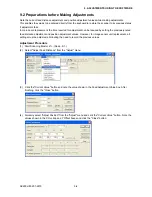
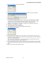
(5) Select All in Calibration and click the Execute button.
(6) The following message is displayed. Insert the calibration sheet into the scanner as instructed.
(7) Click the OK button to start scanning.
The scanned data is displayed when scanning is complete. Colors may differ slightly for individual
sensors to make it easier to identify problem areas in calibration. This does not indicate a defect.
Check that there are no vertical streaks, such as white patches, in the scanned data.
(Streaks occur when calibration is not performed correctly due to contamination by dust or dirt.)
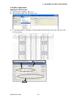
(8) If the data is normal, calibration is complete.
Click the Close button and exit calibration mode.
(9) If any abnormal data is observed, specify the problem areas as follows:
Select Specified Part in Calibration.
(10) The mouse arrow cursor changes to a cross cursor when moved over the data. Click the left mouse
button with the mouse positioned over the streak data. The selected area is shown in blue. Repeat this
procedure for any additional streaks.
Areas that have been selected (shown in blue) can be deselected by clicking the left mouse button
again. To deselect all selected areas, click the Clear button.
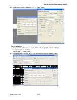
(11) Once all required areas have been specified, remove the calibration sheet and clean the contact glass
plate and scanning-table surfaces. Check the calibration sheet for dust and dirt, then click the Execute
button.
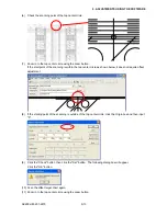
(12) Return to step (5) and verify the calibration results.
Summary of Contents for SK200-09
Page 1: ...SK200 UM251 03 9370 SERVICE MANUAL MANUAL NO SK200 UM 251 ...
Page 6: ......
Page 10: ...SK200 UM 251 9370 1 4 1 OVERVIEW When the scanner is mounted on the high stand 1185 720 1100 ...
Page 38: ......
Page 40: ......
Page 42: ......
Page 100: ......
Page 112: ......
Page 135: ...SK200 UM 251 9370 13 23 13 BLOCK DIAGRAM AND CIRCUIT DIAGRAMS Power Board CN4091 07 2 4 ...
Page 136: ...SK200 UM 251 9370 13 24 13 BLOCK DIAGRAM AND CIRCUIT DIAGRAMS Power Board CN4091 07 3 4 ...
Page 137: ...SK200 UM 251 9370 13 25 13 BLOCK DIAGRAM AND CIRCUIT DIAGRAMS Power Board CN4091 07 4 4 ...
Page 162: ...SK200 UM 251 9370 13 50 13 BLOCK DIAGRAM AND CIRCUIT DIAGRAMS Power Board CN4091 17A 2 4 ...
Page 163: ...SK200 UM 251 9370 13 51 13 BLOCK DIAGRAM AND CIRCUIT DIAGRAMS Power Board CN4091 17A 3 4 ...
Page 164: ...SK200 UM 251 9370 13 52 13 BLOCK DIAGRAM AND CIRCUIT DIAGRAMS Power Board CN4091 17A 4 4 ...


