Freescale Semiconductor PowerQUICC III MPC8541E Manuallines Download Page 5

PowerQUICC III MPC8555E and MPC8541E Bring-Up Guidelines, Rev. 5

Freescale Semiconductor

5


Power

NOTE

From a system standpoint, if the I/O power supplies ramp prior to the V

DD


core supply, then the port pins on the MPC8555E and MPC8541E CPMs 
may drive a logic-one or -zero during power-up.

Table 2

 lists the current maximum ratings for the power supplies. Supplies must not exceed these absolute 

maximum ratings. However, during normal operation, use of the Recommended Operating Conditions 
table in the hardware specification is recommended. Any information in the relevant hardware 
specification supersedes information in 

Table 2

.

2.4

Power Planes

Each V

DD

 pin should be provided with a low-impedance path to the board power supply. Similarly, each 

ground pin should be provided with a low-impedance path to ground. The power supply pins drive distinct 
groups of logic on-chip. The capacitor leads and associated printed circuit traces connecting to chip V

DD


and ground should be kept to less than half an inch per capacitor lead.

2.5

Decoupling

Due to large address and data buses and high operating frequencies, the PowerQUICC III can generate 
transient power surges and high-frequency noise in its power supply, especially while driving large 
capacitive loads. This noise must be prevented from reaching other components in the PowerQUICC III 
system, and the PowerQUICC III itself requires a clean, tightly regulated source of power. Therefore, you 
should place at least one decoupling capacitor at each V

DD

, GV

DD

, LV

DD

, OV

DD

, and pins of the 

PowerQUICC III. These decoupling capacitors should receive their power from separate V

DD

, GV

DD

LV

DD

, OV

DD

, and GND power planes in the PCB, utilizing short traces to minimize inductance. 

Capacitors may be placed directly under the device using a standard escape pattern. Others may surround 
the part. These capacitors should have a value of 0.01 or 0.1 µF. To minimize lead inductance, only ceramic 
SMT (surface mount technology) capacitors should be used. In addition, several bulk storage capacitors 
should be distributed around the PCB, feeding the V

DD

, GV

DD

, LV

DD

, and OV

DD

 planes, to enable quick 

recharging of the smaller chip capacitors. These bulk capacitors should have a low equivalent series 
resistance (ESR) rating to ensure the quick response time necessary. They should also be connected to the 
power and ground planes through two vias to minimize inductance. Suggested bulk capacitors—100–330 
µF. Simulation is strongly recommended to minimize noise on the power supplies before proceeding into 
the PCB design and manufacturing stage of development.

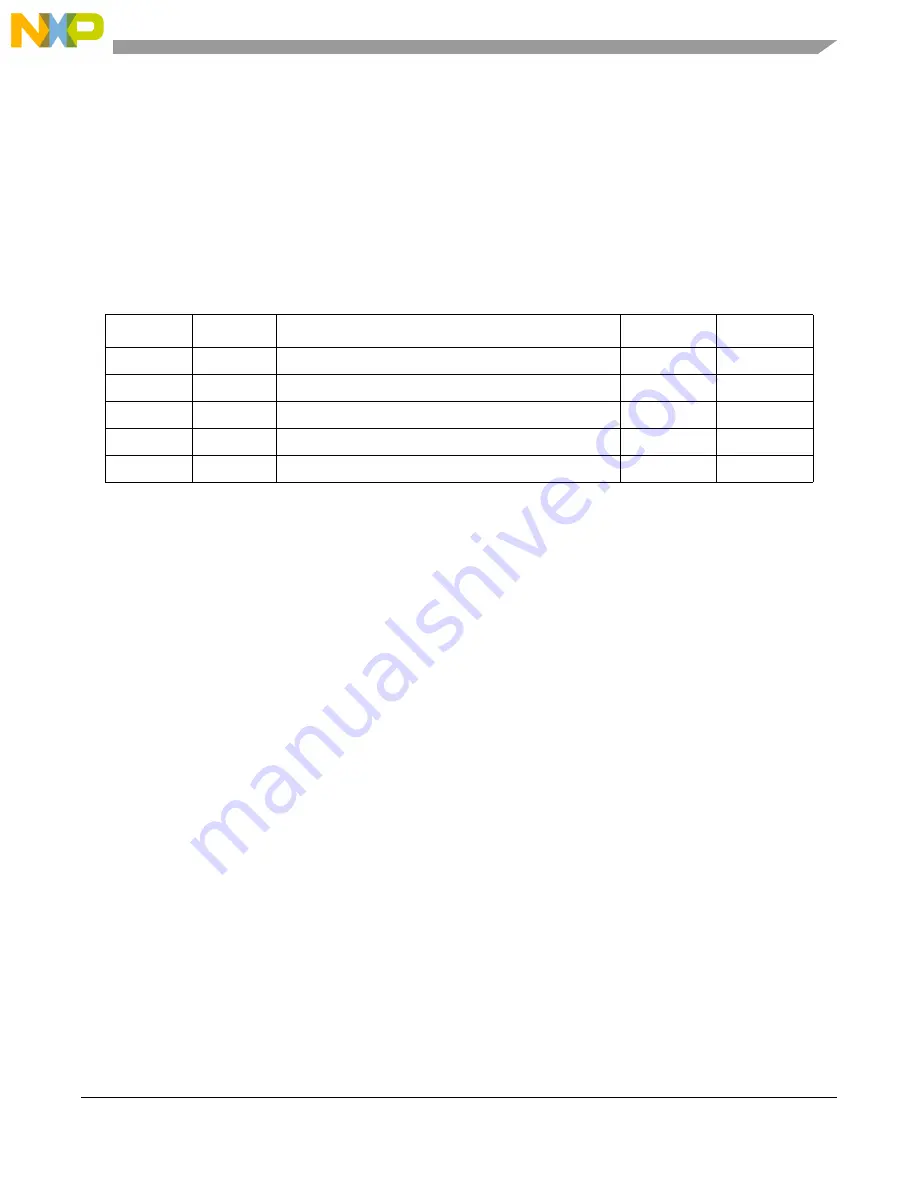
Table 2. Maximum Voltage Ratings

Type

Name

Block

(V)

(Vmax)

Core

Vdd

1.2

1.32

PLL

AVdd

Core PLL, Platform PLL, CPM PLL, PCI1, PCI2

1.2

1.32

I/O

GVdd

DDR

2.5

3.63

I/O

LVdd

TSEC

2.5 / 3.3

2.75 / 3.63

I/O

OVdd

CPM, LBIU, DMA, MII-mgt, PIC1,PCI2, 

I

2

C

3.3

3.63

Summary of Contents for PowerQUICC III MPC8541E

Page 1: ...he aspects of a design that merit special attention during initial system startup 1 Getting Started This section outlines recommendations to simplify the first phase of design Before designing a syste...

Page 2: ...e respective PowerQUICC III device 1 3 Communications Processor Module CPM Performance and Bus Utilization Tool The PowerQUICC III CPM runs by time sharing multiple communication protocols To estimate...

Page 3: ...Tool is available on the MPC8555E or MPC8541E device web site 1 7 Available Training Our third party partners are part of an extensive Design Alliance Program Our current training partners are listed...

Page 4: ...supply the type of load on each power supply and the way different voltages are derived The MPC8555E and MPC8541E require the power rails to be applied in a specific sequence to ensure proper device o...

Page 5: ...ponents in the PowerQUICC III system and the PowerQUICC III itself requires a clean tightly regulated source of power Therefore you should place at least one decoupling capacitor at each VDD GVDD LVDD...

Page 6: ...from the capacitors to the AVDD pin which is on the periphery of the 783 FC PBGA footprint without the inductance of vias If possible a separate plane for each PLL filtering circuit is recommended 3 C...

Page 7: ...ion Core including L1 CCB 2 2 5 3 3 5 DDR CCB 2 I2 C CCB I2CFDR ratio L2 cache CPM CCB Local Bus CCB 2 4 8 Core PLL Platform PLL DLL LSYNC_IN LSYNC_OUT LCLK0 LCLK1 core_clk e500 Core CCB_clk to Rest o...

Page 8: ...nt product web site for updated options 3 3 Core Clock The frequency of the core is determined at POR through the LALE and the LGPL2 pins Below are the options for configuring the core clock as a mult...

Page 9: ...terfaces on the MPC8555E and the MPC8541E is by default the system clock SYSCLK input In asynchronous mode each PCI PCI1 PCI2 interface can be configured to use a separate PCI clock input unrelated to...

Page 10: ...4 1 TRST TRST is the reset pin for the JTAG COP interface It must be held at a low level during the assertion of HRESET to reset all logic completely on the PowerQUICC III For compatibility with thir...

Page 11: ...Connector Physical Pinout 1 2 NC SRESET 2 Populate this with a 10 resistor for short circuit current limiting protection NC OVDD 10 k 10 k HRESET1 to fully control the processor as shown here 4 Altho...

Page 12: ...o that it is asserted when the system reset signal HRESET is asserted ensuring that the JTAG scan chain is initialized during Table 6 COP Header Definition Header Position Name Description 1 COP_TDO T...

Page 13: ...rally output pins during normal operation they are treated as inputs while HRESET is asserted HRESET must be asserted for a minimum of 100 s When HRESET negates the configuration pins are sampled and...

Page 14: ...ins LAD 0 31 to software For example we can pass information about a circuit board revision number to software by driving the pins in any order The information is automatically sampled from LAD 0 31 d...

Page 15: ...41EEC 5 3 Boot Sequencer The boot sequencer allows configuration of any memory mapped register before the boot up code runs When enabled it loads code from an EEPROM on the I2C bus This code can be us...

Page 16: ...are not used it would be more power efficient to disable these interfaces The device disable register DEVDISR contains disable bits for the PCI1 PCI2 LBC SEC L2 DDR e500 Time Base CPM DMA TSEC1 TSEC2...

Page 17: ...neration of PowerQUICC devices Freescale strongly recommends that use of these instructions be confined to libraries and device drivers Customer software that uses SPE or SPFP APU instructions at the...

Page 18: ...s high through a resistor Recommended resistor values are 2 10 k 6 5 Local Bus Interface Unit The local bus frequency can be adjusted through the LCRR CLKDIV bit If modified the DLL requires a re lock...

Page 19: ...K 6 5 3 Timing Local bus output valid hold and tri state timings can be adjusted at reset by the POR pins TSEC2_TXD 6 5 These pins directly affect local bus AC timing by adding up to three buffer del...

Page 20: ...hese internal pull ups are not enabled in 64 bit mode If there is concern that in 32 bit mode these inputs may see noise that would cause unwanted power consumption then external pull up resistors can...

Page 21: ...of the device pins Instead the PCI CLK is realized on the SYSCLK input and the PCI RST is realized on the HRESET input 6 7 Three Speed Ethernet Controller TSEC The TSEC has one management interface th...

Page 22: ...en 2 10 K In general inputs can be tied together to a single resistor I Os must be tied off with a single resistor per I O except on the PCI interface see Section 6 6 PCI Note that if you are not usin...

Page 23: ...ied Section 2 3 Power Sequencing Modified signal names in Table 6 2 6 2006 Updates are as follows Modified note in Section 6 3 DDR SDRAM to clarify that while MSYNC_IN mube connected to MSYNC_OUT the...

Page 24: ...and actual performance may vary over time All operating parameters including typicals must be validated for each customer application by customer s technical experts Freescale does not convey any lic...

Reviews: