Freescale Semiconductor FlexRay MFR4310 Reference Manual Download Page 166

FlexRay Module (FLEXRAYV4)

MFR4310 Reference Manual, Rev. 2

166

Freescale Semiconductor


NOTE

If the number of the last slot in the current communication cycle on a given 
channel is 

n

, all receive message buffers assigned to this channel with 

MBFIDRn.FID greater than

n

 are not updated at all.

When the receive message buffer update has finished the status updated transition 

SU

 is triggered, which 

changes the buffer state from 

CCSu 

to 

Idle

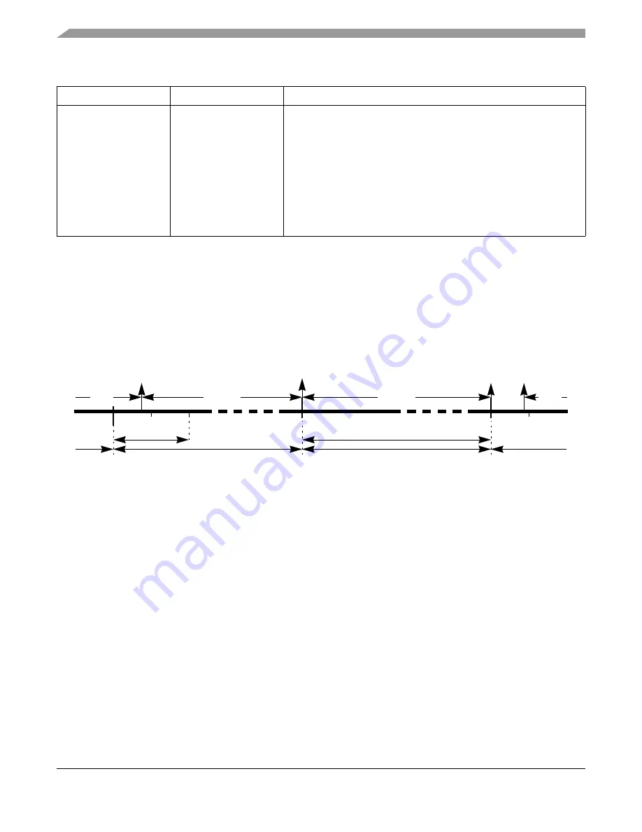
. An example receive message buffer timing and state change 

diagram for a normal frame reception is given in 

Figure 3-119

.

Figure 3-119. Message Reception Timing

The amount of message data written into the message buffer data field of the receive shadow buffer is 
determined by the following two items:

1. the message buffer segment that the message buffer is assigned to, as defined by the 

Message 

Buffer Segment Size and Utilization Register (MBSSUTR)

.

2. the message buffer data field size, as defined by the related field of the 

Message Buffer Data Size 

Register (MBDSR)

3. the number of bytes received over the FlexRay bus

If the message buffer is assigned to the message buffer segment 1, and the number of received bytes is 
greater than 2*MBDSR.MBSEG1DS, the FlexRay module writes only 2*MBDSR.MBSEG1DS bytes 
into the message buffer data field of the receive shadow buffer. If the number of received bytes is less than 
2*MBDSR.MBSEG1DS, the FlexRay module writes only the received number of bytes and does not 
change the trailing bytes in the message buffer data field of the receive shadow buffer. The same holds for 
the message buffer segment 2 with MBDSR.MBSEG2DS.

0

x

No valid frame received.
- Message Buffer Data Field not updated.
- Frame Header Field not updated.
- Slot Status Field updated.
- DUP:= 0
- DVAL not changed.
- MBIF:= 1, if the slot was not an empty dynamic slot.
Note: An empty dynamic slot is indicated by the following frame and slot 

status bit values:

vSS!ValidFrame

 = 0 and 

vSS!SyntaxError

 = 0 and 

vSS!ContentError

 = 0 and 

vSS!BViolation

 = 0.

Table 3-100. Receive Message Buffer Update (Continued)

vSS!ValidFrame

vRF!Header!NFIndicator

Update description

search[s+1]

MT st

art

BS 

slot s

SLS 

SU 

CCBs CCRx 

slot s+1

Idle 

MT star

t

Idle 

slot s+2

slot s

tart

slot s

tart

MT st

art

message receive to receive shadow buffer

SSS 

CCSu 

slot

 st

art

Summary of Contents for FlexRay MFR4310

Page 1: ...FlexRay Communication freescale com Controllers MFR4310RM Rev 2 03 2008 MFR4310 Reference Manual...

Page 2: ......

Page 3: ...MFR4310 Reference Manual MFR4310RM Rev 2 03 2008...

Page 4: ...zes changes made to this document Revision History Date Revision Level Description 9 May 2007 0 First public release 20 Jun 2007 1 Added row for 1M63J maskset to Table 2 2 Changed Figure 4 2 read and...

Page 5: ...Device Overview FlexRay Module FLEXRAYV4 Port Integration Module PIM Dual Output Voltage Regulator VREG3V3V2 Clocks and Reset Generator CRG Oscillator OSCV2 Electrical Characteristics Package Informa...

Page 6: ...MFR4310 Reference Manual Rev 2 6 Freescale Semiconductor...

Page 7: ...Functions and Signal Properties 35 2 4 3 Detailed Signal Descriptions 38 2 4 4 Power Supply Pins 44 2 5 Modes of Operation 45 2 6 External Clock and Host Interface Selection 45 2 6 1 External 4 10 40...

Page 8: ...dual Message Buffer Reconfiguration 178 3 4 9 Receive FIFO 179 3 4 10 Channel Device Modes 184 3 4 11 External Clock Synchronization 186 3 4 12 Sync Frame ID and Sync Frame Deviation Tables 186 3 4 13...

Page 9: ...scription 219 5 2 1 VDDR VSSR Regulator Power Input 219 5 2 2 VDDA VSSA Regulator Reference Supply 219 5 2 3 VDD2_5 VSS2_5 Regulator Output1 Core Logic 220 5 2 4 VDDOSC VSSOSC Regulator Output2 OSC 22...

Page 10: ...k Monitor CM 236 7 5 Resets 236 Appendix A Electrical Characteristics A 1 General 237 A 1 1 Parameter Classification 237 A 1 2 Power Supply 238 A 1 3 Pins 238 A 1 4 Current Injection 238 A 1 5 Absolut...

Page 11: ...nce Manual Rev 2 Freescale Semiconductor 11 Section Number Title Page Appendix B Package Information B 1 64 pin LQFP package 257 Appendix C Printed Circuit Board Layout Recommendations Appendix D Inde...

Page 12: ...MFR4310 Reference Manual Rev 2 12 Freescale Semiconductor Section Number Title Page...

Page 13: ...gister MCR 70 Figure 3 4 Strobe Signal Control Register STBSCR 72 Figure 3 5 Message Buffer Data Size Register MBDSR 75 Figure 3 6 Message Buffer Segment Size and Utilization Register MBSSUTR 76 Figur...

Page 14: ...mer 1 Cycle Set Register TI1CYSR 106 Figure 3 38 Timer 1 Macrotick Offset Register TI1MTOR 106 Figure 3 39 Timer 2 Configuration Register 0 TI2CR0 107 Figure 3 40 Timer 2 Configuration Register 1 TI2C...

Page 15: ...10 125 Figure 3 72 Protocol Configuration Register 11 PCR11 125 Figure 3 73 Protocol Configuration Register 12 PCR12 126 Figure 3 74 Protocol Configuration Register 13 PCR13 126 Figure 3 75 Protocol C...

Page 16: ...er Slot Status Structure ChB 148 Figure 3 108 Message Buffer Data Field Structure 150 Figure 3 109 Single Transmit Message Buffer Access Regions 153 Figure 3 110 Single Transmit Message Buffer States...

Page 17: ...re 3 142 Scheme of combined interrupt flags 201 Figure 4 1 Part ID Register PIDR 210 Figure 4 2 ASIC Version Number Register AVNR for Maskset 1M63J 210 Figure 4 3 Host Interface Pins Drive Strength Re...

Page 18: ...Figure A 3 AMI Interface Write Timing Diagram 251 Figure A 4 MPC Interface Read Timing Diagram 253 Figure A 5 MPC Interface Write Timing Diagram 253 Figure A 6 HCS12 Interface Read Timing Diagram 255...

Page 19: ...10 HCS12 Access Types 53 Table 3 1 List of Terms 59 Table 3 2 External Signal Properties 64 Table 3 3 FlexRay Memory Map 65 Table 3 4 Register Access Conventions 68 Table 3 5 Additional Register Reset...

Page 20: ...Table 3 36 SFCNTR Field Descriptions 100 Table 3 37 SFTOR Field Description 101 Table 3 38 SFTCCSR Field Descriptions 101 Table 3 39 SFIDRFR Field Descriptions 102 Table 3 40 SFIDAFVR Field Descriptio...

Page 21: ...TXSLBR Field Descriptions 121 Table 3 73 Protocol Configuration Register Fields 121 Table 3 74 Wakeup Channel Selection 123 Table 3 75 MBCCSRn Field Descriptions 130 Table 3 76 MBCCFRn Field Descripti...

Page 22: ...age Buffer State Description Transmit Side 171 Table 3 104 Double Transmit Message Buffer Host Transitions 172 Table 3 105 Double Transmit Message Buffer Module Transitions 173 Table 3 106 Double Tran...

Page 23: ...lation Details 243 Table A 6 5V I O Characteristics VDD5 5V 244 Table A 7 3 3V I O Characteristics VDD5 3 3V 245 Table A 8 Supply Current Characteristics 246 Table A 9 Voltage Regulator Operating Cond...

Page 24: ...MFR4310 Reference Manual Rev 2 24 Freescale Semiconductor Table Number Title Page...

Page 25: ...reader understands FlexRay protocol functionality and microcontroller system design 1 2 Additional Reading For additional reading that provides background to or supplements the information in this man...

Page 26: ...12 Freescale s HCS12 family of microcontrollers HIF Host Interface LUT Look Up Table MBIDX Message Buffer Index MBNum Message Buffer Number MCU Microcontroller Unit MPC Device title prefix for Freesca...

Page 27: ...in its inactive logic state An active low signal changes from low to high when deasserted an active high signal changes from high to low when deasserted set To set a bit means to establish logic leve...

Page 28: ...Introduction MFR4310 Reference Manual Rev 2 28 Freescale Semiconductor...

Page 29: ...ssage buffer header status and payload data are stored in FlexRay memory Consistent data access ensured by means of buffer locking scheme Host can lock multiple buffers at the same time Size of messag...

Page 30: ...terfaces HCS12 Interface for direct connection to Freescale s HCS12 family of microcontrollers with interface clock signal to synchronize the data transfer the maximum frequency of this clock signal c...

Page 31: ...PA2 D6 PA1 D7 PA0 D8 PB7 D9 PB6 D10 PB5 D11 PB4 D12 PB3 D13 PB2 D14 PB1 D15 PB0 External Bus Interface AMI HCS12 Interface A1 XADDR19 A2 XADDR18 A3 XADDR17 A4 XADDR16 A5 XADDR15 A6 XADDR14 A7 A8 A9 OE...

Page 32: ...on Register 2 0x0086 0x008A FlexRay Receive FIFO Configuration 6 0x008C 0x008E FlexRay Receive FIFO Status 4 0x0090 0x009A FlexRay Receive FIFO Filter 12 0x009C 0x009E FlexRay Dynamic Segment Status R...

Page 33: ...umber in binary coded decimal Bits 15 to 8 of the MVR comprise the controller host interface CHI version number bits 7 to 0 comprise the protocol engine PE version number These read only values provid...

Page 34: ...9 PB6 D10 PB5 D11 PB4 D12 PB3 D13 PB2 D14 PB1 D15 PB0 VDDX1 VSSX1 A1 XADDR19 A2 XADDR18 A3 XADDR17 A4 XADDR16 A5 XADDR15 RESET INT_CC CLKOUT D8 PB7 D7 PA0 VSS2_5 VDD2_5 D6 PA1 D5 PA2 D4 PA3 D3 PA4 VDD...

Page 35: ...ess bus HCS12 expanded address lines 17 A6 XADDR14 VDDX I PC AMI MPC address bus HCS12 expanded address lines 18 A7 VDDX I PC AMI MPC address bus 21 A8 VDDX I PC AMI MPC address bus 22 A9 VDDX I PC AM...

Page 36: ...s HCS12 multiplexed address data bus 55 D3 PA4 VDDX I O Z DC PC Z AMI MPC data bus HCS12 multiplexed address data bus 51 D2 PA5 VDDX I O Z DC PC Z AMI MPC data bus HCS12 multiplexed address data bus 4...

Page 37: ...DDX I O DC PD Debug strobe point Output clock select 46 DBG3 CLK_S1 VDDX I O DC PD Debug strobe point Output clock select Oscillator 24 EXTAL CLK_CC VDDOSC I Crystal driver External clock 25 XTAL I Cr...

Page 38: ...active low 2 Acronyms PC Pullup pulldown Controlled Register controlled internal weak pullup pulldown for a pin in the input mode Refer to the following sections for more information Section 4 3 1 5...

Page 39: ...he IF_SEL 1 0 pins Refer to Section 2 7 External Host Interface for more information The pins can be configured to enable or disable pullup or pulldown resistors on the pins A 12 11 are AMI MPC interf...

Page 40: ...gured to enable or disable a pullup or pulldown resistor on the pin CE is an AMI MPC interface transfer size input signal It indicates the size of the requested data transfer in the current bus cycle...

Page 41: ...drive TXD_BG 1 2 are bus driver transmit data output signals if the FlexRay Optical Electrical PHY is configured TXD_BG1 is the output of the CC to Physical Layer Channel 1 TXD_BG2 is the output of th...

Page 42: ...The CRG has a built in RESET glitch filter to prevent glitches on the RESET pin from resetting the device see Section 6 4 1 4 RESET Glitch Filter 2 4 3 17 INT_CC Interrupt Output INT_CC is an AMI MPC...

Page 43: ...s See also Chapter 7 Oscillator OSCV2 2 4 3 21 XTAL Crystal Driver Pin XTAL is a crystal driver pin Refer to Figure 2 3 for oscillator connections and Figure 2 4 for external clock connections See als...

Page 44: ...O drivers and input to the internal voltage regulator NOTE The VDDR pin enables the internal 3 3 V to 2 5 V voltage regulator If this pin is tied to ground the internal voltage regulator is turned of...

Page 45: ...de operating voltage and ground for the oscillator This allows the supply voltage to the oscillator to be bypassed independently This 2 5 V voltage is generated by the internal voltage regulator NOTE...

Page 46: ...ces on IF_SEL1 and IF_SEL0 are enabled only during reset they are disabled after the reset operation is complete NOTE The following steps must be taken to select a correct external host interface mode...

Page 47: ...the help of the chip select signal CE and the address lines A 12 1 The AMI interface accepts only aligned 16 bit read and 8 bit or 16 bit write transactions The AMI interface does not support 8 bit re...

Page 48: ...or the AMI D0 is the LSB of the 16 bit data bus NOTE If the AMI mode without the CHICLK_CC signal is selected i e IF_SEL 1 0 0b01 CHICLK_CC must be driven to logic 0 or logic 1 it must not be left flo...

Page 49: ...nductor 49 2 7 1 1 Asynchronous Memory Interface with S12X Family Figure 2 5 AMI Interface with S12X Family MFR4310 S12X Family D0 D15 D15 D0 A1 A12 A12 A1 CE WE OE CSn WE RE BSEL1 UDS LDS BSEL0 INT_C...

Page 50: ...have the meanings shown in Table 2 9 Data exchange in MPC mode is controlled by the CE BSEL 1 0 and OE inputs The MPC interface is implemented as an asynchronous memory slave module thus enabling the...

Page 51: ...OTE D0 is the LSB of the 16 bit data bus Table 2 9 MPC Interface Access Types CE OE BSEL1 BSEL0 Type of Access 0 0 X 0 illegal 0 0 0 X illegal 0 0 1 1 16 bit read from word address1 1 Read data from e...

Page 52: ...expanded address signals XADDR 14 19 are compared with logical 0 s the HCS12 External Bus Interface EBI is in the Paged or Unpaged mode The three most significant bits of the demultiplexed address bu...

Page 53: ...R13 matches ACS0 ADR12 matches ACS1 etc and the address XADDR 14 19 matches 0 The HCS12 interface accepts only aligned 16 bit read and 8 bit or 16 bit write transactions The HCS12 interface does not s...

Page 54: ...or logic 1 i e they must not be left floating Figure 2 8 HCS12 Interface Address Decoding and Internal Chip Select Generation 16 bit Address Data Multi plexer 16 bit 16 bit 10 bit 3 bit 3 bit 6 bit 6...

Page 55: ...with HCS12 Page Mode Support Figure 2 9 HCS12 interface with HCS12 Page Mode Support MFR4310 HCS12 family PB0 PA7 ADDR DATA0 PB0 ECLK_CC LSTRB RW_CC ECLK LSTRB R W INT_CC TXD_BG2 IF_SEL0 TXD_BG1 IF_S...

Page 56: ...e Timing See Section A 6 HCS12 Interface Timing for timing characteristics of the HCS12 interface 2 8 Resets and Interrupts 2 8 1 Resets MFR4310 has the following resets External hard reset input sign...

Page 57: ...changed to known startup states Refer to the respective module chapters for information on the different kinds of resets and for register reset states 2 8 1 1 I O Pin States After Reset Refer to Tabl...

Page 58: ...Device Overview MFR4310 Reference Manual Rev 2 58 Freescale Semiconductor...

Page 59: ...ontroller 0 ppm EBI External Bus Interface FRM FlexRay Memory Memory to store message buffer payload header and status and to store synchronization frame related tables FSS Frame Start Sequence HIF Ho...

Page 60: ...active 3 1 4 Overview The FlexRay module is a FlexRay communication controller that implements the FlexRay Communications System Protocol Specification Version 2 1 Rev A The FlexRay module has three...

Page 61: ...ed and the slot status information are stored in the FlexRay Memory FRM The clock domain crossing unit implements signal crossing from the CHI clock domain to the PE clock domain and vice versa to all...

Page 62: ...0 up to 254 bytes two independent message buffer segments with configurable size of payload data section each segment can contain message buffers assigned to the static segment and message buffers ass...

Page 63: ...Ray module configuration bits and fields in the Module Configuration Register MCR The FlexRay module leaves disabled mode when the application sets the FlexRay module enable bit MEN in the Module Conf...

Page 64: ...lock 3 2 1 2 RXD_BG1 Receive Data Channel A The RXD_BG1 signal carries the receive data for channel A from the corresponding FlexRay bus driver 3 2 1 3 TXD_BG1 Transmit Data Channel A The TXD_BG1 sign...

Page 65: ...Register Description The FlexRay module occupies 1280 bytes of address space starting at address 0x0000 3 3 1 Memory Map The complete memory map of the FlexRay module is shown in Table 3 3 Table 3 3...

Page 66: ...ounter Register SFCNTR R 0x0042 Sync Frame Table Offset Register SFTOR R W 0x0044 Sync Frame Table Configuration Control Status Register SFTCCSR R W Sync Frame Filter 0x0046 Sync Frame ID Rejection Fi...

Page 67: ...Shadow Buffer Index Register RSBIR R W Receive FIFO Configuration 0x0086 Receive FIFO Selection Register RFSR R W 0x0088 Receive FIFO Start Index Register RFSIR R W 0x008A Receive FIFO Depth and Size...

Page 68: ...0 PCR0 Protocol Configuration Register 30 PCR30 R W R W 0x00DE 0x00FE Reserved R Message Buffers Configuration Control Status 0x0100 Message Buffer Configuration Control Status Register 0 MBCCSR0 R W...

Page 69: ...ive Shadow Buffer Index Register RSBIR Each of these memory mapped registers provides a SEL field and a WMD bit The SEL field is used to select the internal register The WMD bit controls the write mod...

Page 70: ...defines the global configuration of the FlexRay module 0x0000 15 14 13 12 11 10 9 8 7 6 5 4 3 2 1 0 R CHIVER PEVER W Reset 1 0 0 0 0 1 0 1 0 1 1 0 0 1 1 0 Figure 3 2 Module Version Register MVR Table...

Page 71: ...Table 3 9 10 SFFE Synchronization Frame Filter Enable This bit controls the filtering for received synchronization frames For details see Section 3 4 15 Sync Frame Filtering 0 Synchronization frame f...

Page 72: ...are undefined and should not be assigned to the strobe ports 1 0 0 ports RXD_BG1 TXD_BG1 and TXEN1 not driven by FlexRay module ports RXD_BG2 TXD_BG2 and TXEN1 not driven by FlexRay module PE channel...

Page 73: ...trobe port are combined with a binary OR operation 00 assign selected signal to DBG0 01 assign selected signal to DBG1 10 assign selected signal to DBG2 11 assign selected signal to DBG3 Table 3 12 St...

Page 74: ...of MTS or CAS symbol A pulse 1 TXD_BG1 36 0x24 B TXD_BG2 37 0x25 start of transmission A pulse 1 TXD_BG1 38 0x26 B TXD_BG2 39 0x27 end of transmission A pulse 1 TXD_BG1 40 0x28 B TXD_BG2 41 0x29 stati...

Page 75: ...ot count 4 70 0x46 slot count 5 71 0x47 slot count 6 72 0x48 slot count 7 73 0x49 slot count 8 74 0x4A slot count 9 75 0x4B slot count 10 76 0x4C cycle start pulse 0 MT start 77 0x4D slot start A puls...

Page 76: ...et 0 1 1 1 1 1 1 1 0 1 1 1 1 1 1 1 Figure 3 6 Message Buffer Segment Size and Utilization Register MBSSUTR Table 3 14 MBSSUTR Field Descriptions Field Description 14 8 LAST_MB_SEG1 Last Message Buffer...

Page 77: ...tocol Operation Control Register POCR Table 3 15 POCR Field Descriptions Field Description 15 WME Write Mode External Correction This bit controls the write mode of the EOC_AP and ERC_AP fields 0 Writ...

Page 78: ...he protocol command to the PE immediately While the transfer is running the BSY bit is set 0000 ALLOW_COLDSTART Immediately activate capability of node to cold start cluster 0001 ALL_SLOTS Delayed1 tr...

Page 79: ...ble is equal to 1 13 CHIF CHI Interrupt Flag This flag is set if at least one of the individual CHI error flags in the CHI Error Flag Register CHIERFR is asserted and the chi error interrupt enable GI...

Page 80: ...t message buffers has the MBIF and MBIE flag asserted 1 At least one individual transmit message buffer has the MBIF and MBIE flag asserted 7 MIE Module Interrupt Enable This flag controls if the modu...

Page 81: ...event 1 Internal protocol error detected 13 ILCF_IF Illegal Protocol Configuration Interrupt Flag This flag is set when the protocol engine has detected an illegal protocol configuration parameter set...

Page 82: ...Ray protocol 0 No such event 1 pLatestTx violation occurred on channel B 5 LTXA_IF pLatestTx Violation on Channel A Interrupt Flag This flag is set when the frame transmission on channel A in the dyna...

Page 83: ...e command is not executed For more details see Section 3 7 2 Protocol Control Command Execution 0 No such event 1 Illegal protocol control command detected 13 PECF_IF Protocol Engine Communication Fai...

Page 84: ...ontrols CSA_IF interrupt request generation 0 interrupt request generation disabled 1 interrupt request generation enabled 11 MRC_IE Missing Rate Correction Interrupt Enable This bit controls MRC_IF i...

Page 85: ...art Interrupt Enable This bit controls CYC_IF interrupt request generation 0 interrupt request generation disabled 1 interrupt request generation enabled 0x001E Write Any Time 15 14 13 12 11 10 9 8 7...

Page 86: ...MBU_EF LCK_EF DBL_EF SBCF_EF FID_EF DPL_EF SPL_EF NML_EF NMF_EF ILSA_EF W Reset 0 0 0 0 0 0 0 0 0 0 0 0 0 0 0 0 Figure 3 13 CHI Error Flag Register CHIERFR Table 3 21 CHIERFR Field Descriptions Field...

Page 87: ...g MBU_EF in the CHI Error Flag Register CHIERFR 0 No such event 1 Non utilized message buffer enabled 8 LCK_EF Lock Error Flag This flag is set if the application tries to lock a message buffer that i...

Page 88: ...the static segment with a Preamble Indicator flag PP asserted has its Null Frame indicator flag NF asserted as well In this case the Global Network Management Registers see Network Management Vector R...

Page 89: ...rror indicator bits vSS SyntaxError vSS ContentError vSS BViolation and vSS TxConflict The FlexRay module increments the status error counter by 1 if for a slot or segment at least one error indicator...

Page 90: ...ns Sheet 1 of 2 Field Description 15 14 ERRMODE Error Mode protocol related variable vPOC ErrorMode This field indicates the error mode of the protocol 00 ACTIVE 01 PASSIVE 10 COMM_HALT 11 reserved 13...

Page 91: ...rt consistency check 1011 reserved 1100 reserved 1101 POC integration coldstart check 1110 POC coldstart gap 1111 POC coldstart join 2 0 WAKEUP STATUS Wakeup Status protocol related variable vPOC Wake...

Page 92: ...ing cold start path under noise conditions This indicates there was some activity on the FlexRay bus while the FlexRay module was starting up the cluster 0 No such event 1 POC normal active state was...

Page 93: ...BVB Symbol Window Boundary Violation on Channel B protocol related variable vSS BViolation for symbol window on channel B This status bit is set if there was some media activity on the FlexRay bus cha...

Page 94: ...symbol window on channel A 0 No such event 1 Syntax error detected 4 MTA Media Access Test Symbol MTS Received on Channel A protocol related variable vSS ValidMTS for symbol window on channel A This...

Page 95: ...ror has been detected on channel B Syntax errors are detected in the communication slots the symbol window and the NIT 0 No syntax error detected 1 Syntax errors detected 8 AVFB Aggregated Valid Frame...

Page 96: ...A 0 No syntactically valid frames received 1 At least one syntactically valid frame received 0x0030 15 14 13 12 11 10 9 8 7 6 5 4 3 2 1 0 R 0 0 MTCT W Reset 0 0 0 0 0 0 0 0 0 0 0 0 0 0 0 0 Figure 3 21...

Page 97: ...0 0 SLOTCNTA W Reset 0 0 0 0 0 0 0 0 0 0 0 0 0 0 0 0 Figure 3 23 Slot Counter Channel A Register SLTCTAR Table 3 31 SLTCTAR Field Descriptions Field Description 10 0 SLOTCNTA Slot Counter Value for Ch...

Page 98: ...ection term due to a lack of synchronization frames the RATECORR value is not updated 0x003A Additional Reset RUN Command 15 14 13 12 11 10 9 8 7 6 5 4 3 2 1 0 R OFFSETCORR W Reset 0 0 0 0 0 0 0 0 0 0...

Page 99: ...t Flag Register 0 PIFR0 or Protocol Interrupt Flag Register 1 PIFR1 is equal to 1 0 All individual protocol interrupt flags are equal to 0 1 At least one of the individual protocol interrupt flags is...

Page 100: ...SFODB SFODA W Reset 0 0 0 0 0 0 0 0 0 0 0 0 0 0 0 0 Figure 3 28 Sync Frame Counter Register SFCNTR Table 3 36 SFCNTR Field Descriptions Field Description 15 12 SFEVB Sync Frames Channel B even cycle p...

Page 101: ...dd cycle tables 0 No effect 1 Triggers lock unlock of the odd cycle tables 13 8 CYCNUM Cycle Number This field provides the number of the cycle in which the currently locked table was recorded If none...

Page 102: ...te only one pair of enabled Sync Frame Tables into FlexRay memory 1 SDVEN Sync Frame Deviation Table Enable This bit controls the generation of the Sync Frame Deviation Tables The application must set...

Page 103: ...t 0 0 0 0 0 0 0 0 0 0 0 0 0 0 0 0 Figure 3 32 Sync Frame ID Acceptance Filter Value Register SFIDAFVR Table 3 40 SFIDAFVR Field Descriptions Field Description 9 0 FVAL Filter Value This field defines...

Page 104: ...h of the network management vector in bytes Table 3 42 NMVR 0 5 Field Descriptions Field Description 15 0 NMVP Network Management Vector Part The mapping between the Network Management Vector Register...

Page 105: ...eld Description 13 T2_CFG Timer T2 Configuration This bit configures the timebase mode of Timer T2 0 T2 is absolute timer 1 T2 is relative timer 12 T2_REP Timer T2 Repetitive Mode This bit configures...

Page 106: ...he value in this register while the timer is running the change becomes effective immediately and timer T1 expires according to the changed value 0x005C Write Any Time 15 14 13 12 11 10 9 8 7 6 5 4 3...

Page 107: ...timer has expired according to the old values 3 3 2 41 Timer 2 Configuration Register 1 TI2CR1 0x0060 Write Any Time 15 14 13 12 11 10 9 8 7 6 5 4 3 2 1 0 R 0 0 T2_CYC_VAL 0 0 T2_CYC_MSK W R T2_MTCNT...

Page 108: ...Selection Register SSSR This register is used to access the four internal non memory mapped slot status selection registers SSSR0 to SSSR3 Each internal registers selects a slot or symbol window NIT w...

Page 109: ...al slot status selection registers for access 00 select SSSR0 01 select SSSR1 10 select SSSR2 11 select SSSR3 10 0 SLOTNUMBER Slot Number This field specifies the number of the slot whose status is sa...

Page 110: ...ter is restricted to valid frames only 6 SYF Sync Frame Restriction This bit is used to restrict the counter to received frames with the sync frame indicator bit set to 1 0 The counter is not restrict...

Page 111: ...on 15 VFB Valid Frame on Channel B protocol related variable vSS ValidFrame channel B 0 vSS ValidFrame 0 1 vSS ValidFrame 1 14 SYB Sync Frame Indicator Channel B protocol related variable vRF Header S...

Page 112: ...hannel A protocol related variable vRF Header NFIndicator channel A 0 vRF Header NFIndicator 0 1 vRF Header NFIndicator 1 4 SUA Startup Frame Indicator Channel A protocol related variable vRF Header S...

Page 113: ...eld provides the current value of the Slot Status Counter 0x0080 Write MTE Any Time CYCCNTMSK CYCCNTVAL POC config 15 14 13 12 11 10 9 8 7 6 5 4 3 2 1 0 R MTE 0 CYCCNTMSK 0 0 CYCCNTVAL W Reset 0 0 0 0...

Page 114: ...1 0 R 0 0 SEL 0 0 0 0 RSBIDX W WMD Reset 0 0 0 0 0 0 0 0 0 0 0 0 0 0 0 0 Figure 3 47 Receive Shadow Buffer Index Register RSBIR Table 3 58 RSBIR Field Descriptions Field Description 15 WMD Write Mode...

Page 115: ...ve FIFO Message ID Acceptance Filter Mask Register RFMIAFMR Receive FIFO Frame ID Rejection Filter Value Register RFFIDRFVR Receive FIFO Frame ID Rejection Filter Mask Register RFFIDRFMR Receive FIFO...

Page 116: ...0 0 0 0 Figure 3 50 Receive FIFO Depth and Size Register RFDSR Table 3 62 RFDSR Field Descriptions Field Description 15 8 FIFO_DEPTH FIFO Depth This field defines the depth of the selected receive FIF...

Page 117: ...008E 15 14 13 12 11 10 9 8 7 6 5 4 3 2 1 0 R 0 0 0 0 0 0 0 0 RDIDX W Reset 0 0 0 0 0 0 0 0 0 0 0 0 0 0 0 0 Figure 3 52 Receive FIFO B Read Index Register RFBRIR Table 3 64 RFBRIR Field Descriptions Fi...

Page 118: ...or details on frame ID filtering see Section 3 4 9 5 Receive FIFO filtering 0x0092 Write POC config 15 14 13 12 11 10 9 8 7 6 5 4 3 2 1 0 R MIDAFMSK W Reset 0 0 0 0 0 0 0 0 0 0 0 0 0 0 0 0 Figure 3 54...

Page 119: ...0 0 0 0 0 0 0 0 0 0 0 0 Figure 3 57 Receive FIFO Range Filter Configuration Register RFRFCFR Table 3 69 RFRFCFR Field Descriptions Field Description 15 WMD Write Mode This control bit defines the writ...

Page 120: ...frame ID range filter 0 0 range filter 0 runs as acceptance filter 1 range filter 0 runs as rejection filter 3 F3EN Range Filter 3 Enable This control bit is used to enable and disable the frame ID r...

Page 121: ...nnel B protocol related variable zLastDynTxSlot channel B Number of the last transmission slot in the dynamic segment for channel B If no frame was transmitted during the dynamic segment on channel B...

Page 122: ...ive pAllowPassiveToActive cyclepairs 12 cluster_drift_damping pClusterDriftDamping T 24 comp_accepted_startup_range_a pdAcceptedStartupRange pDelayCompensationChA T 22 comp_accepted_startup_range_b pd...

Page 123: ...meter definitions Table 3 74 Wakeup Channel Selection wakeup_channel Wakeup Channel 0 A 1 B 0x00A0 Write POC config 15 14 13 12 11 10 9 8 7 6 5 4 3 2 1 0 R action_point_offset static_slot_length W Res...

Page 124: ...13 12 11 10 9 8 7 6 5 4 3 2 1 0 R cas_rx_low_max wakeup_symbol_rx_window W Reset 0 0 0 0 0 0 0 0 0 0 0 0 0 0 0 0 Figure 3 65 Protocol Configuration Register 4 PCR4 0x00AA Write POC config 15 14 13 12...

Page 125: ...ocol Configuration Register 8 PCR8 0x00B2 Write POC config 15 14 13 12 11 10 9 8 7 6 5 4 3 2 1 0 R mini slot_ exists sym bol_ win dow_ exists offset_correction_out W Reset 0 0 0 0 0 0 0 0 0 0 0 0 0 0...

Page 126: ...14 13 12 11 10 9 8 7 6 5 4 3 2 1 0 R first_minislot_action_point_offset static_slot_after_action_point W Reset 0 0 0 0 0 0 0 0 0 0 0 0 0 0 0 0 Figure 3 74 Protocol Configuration Register 13 PCR13 0x00...

Page 127: ...15 14 13 12 11 10 9 8 7 6 5 4 3 2 1 0 R wakeup_pattern key_slot_id W Reset 0 0 0 0 0 0 0 0 0 0 0 0 0 0 0 0 Figure 3 79 Protocol Configuration Register 18 PCR18 0x00C6 Write POC config 15 14 13 12 11...

Page 128: ...11 10 9 8 7 6 5 4 3 2 1 0 R micro_per_cycle 15 0 W Reset 0 0 0 0 0 0 0 0 0 0 0 0 0 0 0 0 Figure 3 84 Protocol Configuration Register 23 PCR23 0x00D0 Write POC config 15 14 13 12 11 10 9 8 7 6 5 4 3 2...

Page 129: ...ocol Configuration Register 27 PCR27 0x00D8 Write POC config 15 14 13 12 11 10 9 8 7 6 5 4 3 2 1 0 R dynamic_slot _idle_phase macro_after_offset_correction W Reset 0 0 0 0 0 0 0 0 0 0 0 0 0 0 0 0 Figu...

Page 130: ...er 12 MTD Message Buffer Transfer Direction This bit defines the transfer direction of the message buffer 0 Receive message buffer 1 Transmit message buffer Message Buffer Control 11 CMT Commit for Tr...

Page 131: ...the update conditions 0 message buffer data field contains no valid frame data 1 message buffer data field contains valid frame data Single Transmit Message Buffer Indicates whether the message is tr...

Page 132: ...nment and control the receive and transmit behavior of the message buffer according to Table 3 77 12 CCFE Cycle Counter Filtering Enable This control bit is used to enable and disable the cycle counte...

Page 133: ...The semantic of this field depends on the message buffer transfer type Receive Message Buffer This field is used as a filter value to determine if the message buffer is used for reception of a message...

Page 134: ...rs The physical message buffers are located in the FRM The structure of a physical message buffer is depicted in Figure 3 96 A physical message buffer consists of two fields the message buffer header...

Page 135: ...ield contains the frame payload data or a part of it of the frame to be transmitted to or received from the FlexRay bus The minimum length of this field depends on the specific message buffer configur...

Page 136: ...g the Message Buffer Segment Size and Utilization Register MBSSUTR All individual message buffers with a message buffer number n less than or equal to MBSSUTR LAST_MB_SEG1 belong to the first message...

Page 137: ...n 3 3 The length required for the message buffer data field depends on the message buffer segment that the receive shadow buffer is assigned to For the receive shadow buffers assigned to the first mes...

Page 138: ...1 RFSIR SIDX 10 0x800 Eqn 3 4 The start address SADR_MBHF n of the last message buffer header field that belongs to the receive FIFO in the FRM is determined according to Equation 3 5 SADR_MBHF n RFSI...

Page 139: ...rs and the number of individual message buffers that are used For more details see Section 3 4 3 1 1 Individual Message Buffer Segments Specific Configuration Data The set of message buffer specific c...

Page 140: ...ame ID Rejection Filter Value Register RFFIDRFVR Receive FIFO Frame ID Rejection Filter Mask Register RFFIDRFMR Receive FIFO Range Filter Configuration Register RFRFCFR 3 4 3 7 2 Receive FIFO Control...

Page 141: ..._MBHF i 10 0x800 0 i 256 Eqn 3 7 3 The message buffer header fields for a receive FIFO have to be a contiguous area 3 4 4 2 Message Buffer Data Area The message buffer data area contains all the messa...

Page 142: ...ld A description of the structure of the message buffer header fields is given in Section 3 4 2 1 Message Buffer Header Field Each message buffer header field consists of three sections the frame head...

Page 143: ...se values are generated internally before frame transmission depending on the current transmission state and configuration For transmit message buffers assigned to the static segment the PLDLEN value...

Page 144: ...it and represents the value of the Null Frame Indicator of the first valid frame received on the FlexRay bus in the slot indicated by the CYCCNT field For transmit message buffers the value of this bi...

Page 145: ...of the communication cycle in which the frame stored in this message buffer was received For transmit message buffers the value of this field is ignored The FlexRay module overwrites this value with...

Page 146: ...IFO Channel B Message Buffer see Figure 3 104 15 14 13 12 11 10 9 8 7 6 5 4 3 2 1 0 R VFB SYB NFB SUB SEB CEB BVB CH VFA SYA NFA SUA SEA CEA BVA 0 Reset 15 14 13 12 11 10 9 8 7 6 5 4 3 2 1 0 R 0 0 0 0...

Page 147: ...e first valid frame in the slot This flag is set to 0 if no valid frame was received at all in the subscribed slot 0 first valid frame received on channel A or no valid frame received at all 0 first v...

Page 148: ...10 9 8 7 6 5 4 3 2 1 0 R 0 0 0 0 0 0 0 0 VFA SYA NFA SUA SEA CEA BVA TCA Reset 15 14 13 12 11 10 9 8 7 6 5 4 3 2 1 0 R VFB SYB NFB SUB SEB CEB BVB TCB 0 0 0 0 0 0 0 0 Reset Table 3 85 Transmit Messag...

Page 149: ...annel A protocol related variable vRF Header NFIndicator channel A 0 vRF Header NFIndicator 0 1 vRF Header NFIndicator 1 4 SUA Startup Frame Indicator Channel A protocol related variable vRF Header Su...

Page 150: ...does not update the Message Buffer Data Field For receive FIFOs the application can read the message buffer indicated by the Receive FIFO A Read Index Register RFARIR or the Receive FIFO B Read Index...

Page 151: ...tate The application configures the number of utilized individual message buffers by writing the message buffer number of the last utilized message buffer into the LAST_MB_UTIL field in the Message Bu...

Page 152: ...ed MBCCSRn EDS equals 0 The individual message buffer type is defined by the MTD and MBT bits in the Message Buffer Configuration Control Status Registers MBCCSRn as given in Table 3 89 The message bu...

Page 153: ...3 90 If an region is active as indicated in Table 3 91 the access scheme given for that region applies to the message buffer Figure 3 109 Single Transmit Message Buffer Access Regions The trigger bits...

Page 154: ...e application with the required message buffer status information The internal status information is not visible to the application 3 4 6 2 2 Message Buffer States This section describes the transmit...

Page 155: ...tion has no effect command is ignored and message buffer state is not changed In this case the message buffer lock error flag LCK_EF in the CHI Error Flag Register CHIERFR is set CCSa 1 0 Slot Assigne...

Page 156: ...CKS 0 Application triggers message buffer lock HU MBCCSRn LCKS 1 Application triggers message buffer unlock Table 3 93 Single Transmit Message Buffer Module Transitions Transition Condition Descriptio...

Page 157: ...ge buffer search described in Section 3 4 7 Individual Message Buffer Search the FlexRay module triggers the message available transition MA for up to two transmit message buffers This changes the mes...

Page 158: ...Frame Transmission A static slot with slot number S is assigned to the FlexRay module for channel A if at least one transmit message buffer is configured with the MBFIDRn FID set to S and MBCCFRn CHA...

Page 159: ...sage buffer is unlocked or committed before the transmission slot starts A transmit message buffer timing and state change diagram for null frame transmission for this case is given in Figure 3 115 Fi...

Page 160: ...g is asserted the message buffer is in the state transmission mode In this case each committed message is transmitted as long as the application provides new data or locks the message buffers The Flex...

Page 161: ...the message was received A individual message buffer with message buffer number n is configured as a receive message buffer by the following configuration settings MBCCSRn MBT 0 single buffered messag...

Page 162: ...tes is given in Table 3 91 which also provides the access scheme for the access regions The status bits MBCCSRn EDS and MBCCSRn LCKS provide the application with the required status information The in...

Page 163: ...nsition has no effect command is ignored and message buffer state is not changed In this case the message buffer lock error flag LCK_EF in the CHI Error Flag Register CHIERFR is set HDisLck 0 1 CFG Di...

Page 164: ...ting state is locked buffer subscribed state HLckCCRx 3 4 6 3 2 Message Buffer Search The FlexRay module starts a sequential search that checks all message buffers at the following protocol related ev...

Page 165: ...tatus of the receive message buffers that are the CCRx or HLckCCRx are not modified in the reception slot 3 4 6 3 4 Message Buffer Status Update With the start of the next static or dynamic slot or wi...

Page 166: ...er the FlexRay bus If the message buffer is assigned to the message buffer segment 1 and the number of received bytes is greater than 2 MBDSR MBSEG1DS the FlexRay module writes only 2 MBDSR MBSEG1DS b...

Page 167: ...the identified receive message buffer depending on the slot status and the FlexRay segment the message buffer is assigned to The shadow buffer concept with its index exchange results in the fact that...

Page 168: ...xclusive access to the data control and status bits of the message buffer The access scheme for double transmit message buffers is depicted in Figure 3 121 The given regions represent fields that can...

Page 169: ...3 122 A description of the states is given in Table 3 103 The states for the transmit side of a double transmit message buffer are given in Figure 3 123 A description of the states is given in Table...

Page 170: ...der configuration Commit Side can not be used for internal message transfer CCITx 1 0 ITX Internal Message Transfer Message Buffer Data transferred from commit side to transmit side commit side specif...

Page 171: ...for Null Frame transmission CCSaCCITx 1 0 TX Slot Assigned and Internal Message Transfer Message buffer assigned to next static slot and Message Buffer Data transferred from commit side to transmit s...

Page 172: ...t buffer lock error flag DBL_EF in the CHI Error Flag Register CHIERFR is set The transitions triggered depend on the current value of the LCKS bit The lock and unlock commands only affect the commit...

Page 173: ...specific transitions SA slot match and static slot Slot Assigned Message buffer is assigned to next static slot MA slot match and CycleCounter match Message Available Message buffer is assigned to nex...

Page 174: ...it side CMT bit is cleared the commit side interrupt flag MBIF is set the transmit side CMT bit is set and the transmit side DVAL bit is cleared The conditions and the point in time when the internal...

Page 175: ...de is in the idle state 2 the commit site message data are valid MBCCSR 2n CMT equals 1 3 the transmit side is in one of the states idle CCSa or CCMa It is not checked whether the transmit side contai...

Page 176: ...essage buffer search checks all enabled individual message buffer to determine if a certain slot is assigned to this node for transmission or if this node is subscribed to a certain slot for reception...

Page 177: ...ceive message buffer with a matching frame ID and a matching cycle counter filter appear in the matching message buffer list 3 4 7 1 2 Message Buffer Cycle Counter Filtering The message buffer cycle c...

Page 178: ...assignments occur for one slot An inconsistent channel assignment for message buffer 0 and message buffer 1 is depicted in Figure 3 126 Figure 3 126 Inconsistent Channel Assignment 3 4 8 Individual Me...

Page 179: ...ffer into two single buffers or combines two single buffer into one double buffer In the later case the two single message buffers must have consecutive message buffer numbers and the smaller one must...

Page 180: ...ame reception to the receive FIFO is enabled if for a certain slots no message buffer is assigned or subscribed In this case the FIFO filter path shown in Figure 3 128 is activated When the receive FI...

Page 181: ...lue is provided by the SIDX field in the Receive FIFO Start Index Register RFSIR 3 4 9 5 Receive FIFO filtering The receive FIFO filtering is activated after all enabled individual receive message buf...

Page 182: ...the value mask filter value passes the filter i e is not rejected Consequently a received valid frame with the frame ID FID passes the RX FIFO Frame ID Value Mask Rejection Filter if Equation 3 10 is...

Page 183: ...FCTR FiEN equals 1 Equation 3 11 is fulfilled Eqn 3 11 Consequently all frames with a frame ID that fulfills Equation 3 12 for at least one of the enabled rejection filters is rejected and does not pa...

Page 184: ...are connected to physical FlexRay bus lines The FlexRay port consisting of RXD_BG1 TXD_BG1 and TXEN1 is connected to the physical bus channel A and the FlexRay port consisting of RXD_BG2 TXD_BG2 and...

Page 185: ...hannel B The two FlexRay channels differ only in the initial value for the frame CRC cCrcInit For a single channel device the application can access and configure only the registers related to interna...

Page 186: ...tion Timing If the rate correction for the cycle pair 2n 2 2n 3 shall be affect by the external offset correction the ERC_AP field must be written to after the start of cycle 2n and before the end of...

Page 187: ...hA 11 Sync Frame ID ChA 12 Sync Frame ID ChA 13 Sync Frame ID ChA 14 Sync Frame ID ChA 15 Sync Deviation ChA 1 Sync Deviation ChA 2 Sync Deviation ChA 3 Sync Deviation ChA 4 Sync Deviation ChA 5 Sync...

Page 188: ...Ray module does not update the table in this cycle If this bit is cleared the FlexRay module locks this table and starts the table update To indicate that these tables are currently updated and may co...

Page 189: ...lock the table that is currently written If the application locks the table outside of the table write window the lock is granted immediately 3 4 12 5 1 Sync Frame Table Locking and Unlocking The app...

Page 190: ...header_crc provides header crc for sync frame or startup frame Message buffer with message buffer number n PCR18 key_slot_id The generation of the sync or startup frames depends on the current protoco...

Page 191: ...ization frame did not pass at least one of the two filters this frame is processed as a normal frame and is not considered for clock synchronization 3 4 15 1 Sync Frame Acceptance Filtering The synchr...

Page 192: ...es SEL field only 2 Read STBCSR The SEL field provides N and the ENB and STBPSEL fields provides the settings for signal N 3 4 16 2 Strobe Signal Timing This section provides detailed timing informati...

Page 193: ...titive the T1ST bit is not cleared and the timer is restarted immediately The T1ST is cleared when the timer is stopped 3 4 17 2 Absolute Relative Timer T2 The timer T2 can be configured to be an abso...

Page 194: ...each static slot for each dynamic slot for the symbol window and for the NIT on a per channel base The content of the slot status vector is described in Table 3 109 The PE provides the slot status ve...

Page 195: ...rts for slots in which the module does not transmit vSS TxConflict reception ongoing while transmission starts first valid channel that has received the first valid frame received frame related status...

Page 196: ...counter is incremented if its increment condition defined by the Slot Status Counter Condition Register SSCCR matches the status vector provided by the PE All static slots the symbol window and the N...

Page 197: ...l slot status counter SSCRn_INT is reset at each cycle start If the slot status counter is in the multicycle mode i e SSCCRn MCY equals 1 the counter is not reset and incremented until the maximum val...

Page 198: ...pt enable bit 3 4 19 1 5 CHI Error Interrupts The FlexRay module provides 16 interrupt sources for CHI related error events For details see CHI Error Flag Register CHIERFR There is one common interrup...

Page 199: ...s generated when at least one of the individual chi error interrupt sources generates an interrupt request and the interrupt enable bit GIFER CHIE is set 3 4 19 2 5 Module Interrupt The combined modul...

Page 200: ...0 CHIER 15 0 16 PRTXIRQ 31 16 PIFR0 15 0 16 PRTXIRQ 15 0 PIFR1 15 0 16 RBIRQ CHIIRQ PRTIRQ GIFER FNEAIF FNEAIRQ GIFER WUPIF WUPIRQ GIFER RBIE MBCCSRn MTD Receive Transmit GIFER PRIE GIFER WUPIE GIFER...

Page 201: ...d interrupt flags OR INT_CC MIRQ CRSR LVIF CRSR CMIF CRSR PRIF CRSR ERIF Interrupt Sources Combined Interrupt Flags MBCCSRn MBIF n CHIER 15 0 PIFR0 15 0 PIFR1 15 0 GIFER FNEAIF GIFER WUPIF CIFR TBIF C...

Page 202: ...t rates are implemented by modifying the duration of the microtick pdMicrotick the number of samples per microtick pSamplesPerMicrotick the number of samples per bit cSamplesPerBit and the strobe offs...

Page 203: ...sage buffers used and the message buffer segmentation in the Message Buffer Segment Size and Utilization Register MBSSUTR define the message buffer data size in the Message Buffer Data Size Register M...

Page 204: ...CHI frequency for a selected set of relevant protocol parameters is given in Table 3 111 3 7 Application Information 3 7 1 Shut Down Sequence This section describes a safe shut down sequence to stop t...

Page 205: ...and is not queued and is lost If the command execution block of the PE is idle it selects the next accepted protocol command with the highest priority from the current protocol command vector accordin...

Page 206: ...buffer locks The following sequence must be executed by the application to put the protocol into the POC default config state 1 Repeatedly send Protocol Command FREEZE via Protocol Operation Control R...

Page 207: ...ration Module can be put into the following modes Functional Mode In this mode the module drives each associated pin and has complete control of the direction of that pin The drive strength and pullup...

Page 208: ...s the LSB of the HCS12 address data bus Input Output DC PU PD D 7 0 PA 0 7 AMI MPC data bus HCS12 multiplexed address data bus D0 is the LSB of the AMI MPC data bus PA7 is the MSB of the HCS12 address...

Page 209: ...C_CLK Crystal driver External clock Input XTAL Crystal driver Input 1 Acronyms PC Pullup pulldown Controlled Register controlled internal weak pullup pulldown for a pin in the input mode PU PD Pullup...

Page 210: ...lock pins 0x00FA Host Interface Pins Pullup pulldown Control Register HIPPCR R W 0x00FC Physical Layer Pins Pullup pulldown Enable Register PLPPER R W 0x00FE Physical Layer Pins Pullup pulldown Contro...

Page 211: ...in drive strength is reduced to 1 3 of full strength 1 Pin drive strength is full Address in MFR4310 0x00F6 Write Any Time 15 14 13 12 11 10 9 8 7 6 5 4 3 2 1 0 R 0 0 0 0 0 0 0 0 0 0 0 0 TXD_BG2 TXD_B...

Page 212: ...pullup pulldown enabled 2 A3 XADDR17 AMI MPC address bit 3 HCS12 expanded address bit 17 pullup pulldown enable 0 pullup pulldown disabled 1 pullup pulldown enabled 3 A4 XADDR16 AMI MPC address bit 4...

Page 213: ...FA Write Any Time 15 14 13 12 11 10 9 8 7 6 5 4 3 2 1 0 R 0 0 WE RW_CC CE LSTRB D 0 15 PA 0 7 PB 0 7 A12 ACS2 A11 ACS1 OE ACS0 BSEL 1 0 A 10 7 A6 XADDR14 A5 XADDR15 A4 XADDR16 A3 XADDR17 A2 XADDR18 A1...

Page 214: ...1 pullup 9 A11 ACS1 AMI MPC address bit 11 HCS12 address select bit 1 pullup pulldown control 0 pulldown 1 pullup 10 A12 ACS2 AMI MPC address bit 12 HCS12 address select bit 2 pullup pulldown control...

Page 215: ...interface Host Interface Physical Layer Interface Clock Interface Table 4 8 PLPPER Field Descriptions Field Description 0 RXD_BG1 Receive data channel A pullup pulldown enable 0 pullup pulldown disab...

Page 216: ...e In reset mode the Port Integration Module provides access to four configuration pins for clock output control in the CRG and external bus interface EBI control in the FlexRay IP block In this case t...

Page 217: ...es on MFR4310 Full performance mode FPM The regulator is active providing the nominal supply voltage of 2 5 V with full current sourcing capability at both outputs Features LVR low voltage reset and P...

Page 218: ...erence Manual Rev 2 218 Freescale Semiconductor Figure 5 1 VREG3V3 Block Diagram LVR POR VDDR VDD2_5 POR LVR CTRL VSS2_5 VDDOSC VSSOSC REG REG2 REG1 PIN VDDA VSSA REG Regulator Core CTRL Regulator Con...

Page 219: ...tering shutdown mode pin VDDR must be tied to ground In that case VDD2_5 VSS2_5 and VDDOSC VSSOSC must be provided externally 5 2 2 VDDA VSSA Regulator Reference Supply Signals VDDA VSSA which are sup...

Page 220: ...e is also the regulator control block CTRL which manages the operating modes of VREG3V3V2 5 3 1 REG Regulator Core VREG3V3V2 respectively its regulator core has two parallel independent regulation loo...

Page 221: ...s the reset of the CC The reset values of registers and signals are provided in Section 3 3 Memory Map and Register Description Possible reset sources are listed in Table 5 2 5 4 1 Power On Reset Duri...

Page 222: ...Dual Output Voltage Regulator VREG3V3V2 MFR4310 Reference Manual Rev 2 222 Freescale Semiconductor...

Page 223: ...ality while the CRG is in another operational modes are out of the scope of this documentation 6 1 2 Features The CRG includes the following main features System reset generation from power on and ext...

Page 224: ...t pin with open drain Z Tristated pin 3 No load allowed except for bypass capacitors 4 Reset state All pins with the PC option pullup pulldown is disabled All pins with the DC option have full drive s...

Page 225: ...en a low voltage reset has occurred Cleared by writing a 1 Writing 0 has no effect 1 CMIF Clock Monitor Reset Interrupt Flag set when a clock monitor reset has occurred Cleared by writing a 1 Writing...

Page 226: ...ss a reset event with more priority is detected A reset procedure with the same priority as the currently running one stops the previous procedure and is executed 6 4 1 1 Power on Reset When the power...

Page 227: ...R CMIE bit to 0 asserts the INT_CC interrupt line and sets the low voltage reset interrupt flag CRSR LVIF on the rising edge of the low voltage reset signal The CRG resets the DER CMIE bit to 0 assert...

Page 228: ...ly 70 EXTAL CLK_CC clock periods after the deassertion of the RESET The CRG asserts the INT_CC interrupt line and the external reset interrupt flag CRSR ERIF on the assertion of the RESET signal NOTE...

Page 229: ...on The interface mode selection is done when the TXD_BG 1 2 IF_SEL 1 0 pins are in the IF_SEL 1 0 mode In the TXD_BG 1 2 modes the pads are outputs from the MFR4310 device NOTE The PIM block selects t...

Page 230: ...sets the CRSR ECS bit to 1 otherwise the CRG resets the CRSR ECS bit to 0 6 4 3 CLKOUT Mode Selection and Control The CLKOUT mode selection is done when the DBG 3 2 CLK_S 1 0 pins are in the CLK_S 1...

Page 231: ...ltage clock monitor or external reset process is ongoing The CRG latches the CLK_S 1 0 signal values during the latching window as presented on Figure 6 9 Figure 6 10 and Figure 6 11 The latched value...

Page 232: ...ference Manual Rev 2 232 Freescale Semiconductor Figure 6 10 CLKOUT Mode Selection and Control during External Reset CLK_S 1 0 30 EXTAL CLK_CC periods 60 EXTAL CLK_CC periods Latching window system re...

Page 233: ...anual Rev 2 Freescale Semiconductor 233 Figure 6 11 CLKOUT Mode Selection and Control during Power on Reset CLK_S 1 0 power on reset 16380 EXTAL CLK_CC periods 16410 EXTAL CLK_CC periods Latching wind...

Page 234: ...Clocks and Reset Generator CRG MFR4310 Reference Manual Rev 2 234 Freescale Semiconductor...

Page 235: ...Operation One mode of operation exists Full swing Pierce oscillator mode that can also be used to feed in an externally generated square wave suitable for high frequency operation and harsh environme...

Page 236: ...e connected to a crystal or an external clock source The XTAL pin is an output signal that provides crystal circuit feedback A buffered EXTAL signal OSCCLK becomes the internal reference clock To impr...

Page 237: ...ntroduction is intended to give an overview on several common topics like power supply current injection etc A 1 1 Parameter Classification The electrical parameters shown in this supplement are guara...

Page 238: ...d VDDR pins VDD is used for VDD2_5 and VDDOSC VSS is used for VSS2_5 and VSSOSC IDD is used for the current flowing into VDD2_5 A 1 3 Pins There are four groups of functional pins A 1 3 1 3 3V I O pin...

Page 239: ...d voltages to this high impedance circuit Reliability of operation is enhanced if unused inputs are tied to an appropriate logic voltage level VSS5 or VDD5 Table A 1 Absolute Maximum Ratings Num Ratin...

Page 240: ...temperature followed by hot temperature unless specified otherwise in the device specification Table A 2 ESD and Latch up Test Conditions Model Description Symbol Value Unit Human Body Series Resista...

Page 241: ...sipation W JA Package Thermal Resistance C W Table A 4 Operating Conditions Rating Symbol Min Typ Max Unit Oscillator and Quartz frequency1 1 Input clock frequency applied to EXTAL CLK_CC fOSC 40 40 M...

Page 242: ...ociated with VDDX and VDDR For RDSON is valid Eqn A 5 respectively Eqn A 6 2 Internal voltage regulator enabled Eqn A 7 IDDR is the current shown in Table A 8 and not the overall current flowing into...

Page 243: ...ouble sided PCB with 2 internal planes1 R JMA 42 o C W 5 Junction to Board LQFP642 2 Junction to Board thermal resistance determined per JEDEC JESD51 8 Thermal test board meets JEDEC specification for...

Page 244: ...uA 5 P Output High Voltage pins in output mode 50 Partial Drive IOH 2mA VOH VDD5 0 8 V 6 P Output High Voltage pins in output mode 100 Full Drive IOH 10mA VOH VDD5 0 8 V 7 P Output Low Voltage pins in...

Page 245: ...VDD5 0 4 V 6 P Output High Voltage pins in output mode 100 Full Drive IOH 4 5mA VOH VDD5 0 4 V 7 P Output Low Voltage pins in output mode 50 Partial Drive IOL 0 9mA VOL 0 4 V 8 P Output Low Voltage p...

Page 246: ...measured with internal voltage regulator enabled and a 40 MHz oscillator in standard Pierce mode Production testing is performed using a square wave signal at the EXTAL input Table A 8 Supply Current...

Page 247: ...Unit 1 P Input Voltages VVDDR A 2 97 5 5 V 2 P Regulator Current Shutdown Mode IREG 40 A 3 P Output Voltage Core Full Performance Mode Shutdown Mode VDD 2 45 2 5 1 1 High Impedance Output 2 75 V V 4...

Page 248: ...not scaled A 2 3 Output Loads A 2 3 1 Resistive Loads On chip voltage regulator intended to supply the internal logic and oscillator circuits allows no external DC loads A 2 3 2 Capacitive Loads The...

Page 249: ...are also valid if the device is powered externally After releasing the POR reset the oscillator is started A 3 1 2 LVR The assert level VLVRA see Table A 9 is derived from the VDD supply After releasi...

Page 250: ...ce state when the device is not selected CE is HIGH the outputs are disabled OE HIGH or during a write operation CE LOW and WE LOW Table A 12 Oscillator Characteristics Conditions are shown in Table A...

Page 251: ...agram FUNC1 A 12 1 ADDRESS tSAR D 15 0 DATA tHAR tLZOE tHZOE tHOE tRC tDOE tLOE WE tWEOE tOEWE Note The signal FUNC1 is a logical OR of the chip enable CE and output enable OE inputs FUNC2 A 12 1 ADDR...

Page 252: ...s Over the Operating Range1 1 tAMI_CLK is the period in ns of the CHI and host interface clock selected by IF_SEL 1 0 as described in Table 2 6 Characteristic Symbol Min Max Unit Read Cycle Read Time...

Page 253: ...A 12 1 ADDRESS tSAR D 15 0 DATA tHAR tLZOE tHZOE tHOE tRC tDOE tLOE BSEL 1 0 tBSELOE tOEBSEL Note The signal FUNC3 is a logical OR of the chip enable CE and output enable OE inputs FUNC4 A 12 1 ADDRE...

Page 254: ...LOW time tLOE 2 5 tCHICLK_CC 272 2 Depends on duty cycle of the CHI and host interface clock tLOE 3 0 tCHICLK_CC tCHICLK_CC_HIGH 27 where tCHICLK_CC_HIGH is the period in ns of the high phase of the...

Page 255: ...ce Read Timing Diagram Figure A 7 HCS12 Interface Write Timing Diagram ECLK_CC PA 0 7 PB 0 7 ADDRESS RW_CC tSA ACS 2 0 DATA tHA tLEC tHEC tSRW tDEC tHDR tDRW tHRW tSDR tHDA XADDR 19 14 ADDRESS ECLK_CC...

Page 256: ...f EXTAL CLK_CC and tCLK_CC_HIGH is the period in ns of the high phase of EXTAL CLK_CC ns Address valid time to ECLK_CC rise tSA 11 ns Write Data delay time tDDW 70 ns Write Data hold time tHDW 80 ns R...

Page 257: ...Package Information MFR4310 Reference Manual Rev 2 Freescale Semiconductor 257 Appendix B Package Information B 1 64 pin LQFP package Figure B 1 64 pin LQFP Mechanical Dimensions Case N 840F 02 Page 1...

Page 258: ...Package Information MFR4310 Reference Manual Rev 2 258 Freescale Semiconductor Figure B 2 64 pin LQFP Mechanical Dimensions Case N 840F 02 Page 2...

Page 259: ...Package Information MFR4310 Reference Manual Rev 2 Freescale Semiconductor 259 Figure B 3 64 pin LQFP Mechanical Dimensions Case N 840F 02 Page 3...

Page 260: ...Package Information MFR4310 Reference Manual Rev 2 260 Freescale Semiconductor...

Page 261: ...s possible Occupied board area for C1 C2 C3 and Q should be as small as possible Other signals or supply lines should not be routed under the area occupied by C1 C2 C3 and Q and the connection area of...

Page 262: ...commended PCB Layout 64 pin LQFP for Standard Pierce Oscillator Mode Cload Cd Cd Cd Cd Cd C3 Rs Rb Q C1 C2 VDDX1 VSSX1 VSSR VDDR VSSOSC VDDOSC VSSX4 VDDX4 VSS2_5 VDD2_5 VDDX3 VSSX3 VDDA VSSA Suggested...

Page 263: ...gister GIFER 78 H Host Interface Pins Drive Strength Register HIPDSR 210 Host Interface Pins Pullup down Control Register HIPPCR 213 Host Interface Pins Pullup down Enable Register HIPPER 212 L Last D...

Page 264: ...ister 10 PCR10 125 Protocol Configuration Register 11 PCR11 125 Protocol Configuration Register 12 PCR12 126 Protocol Configuration Register 13 PCR13 126 Protocol Configuration Register 14 PCR14 126 P...

Page 265: ...Index Register RFBRIR 117 Receive FIFO Depth and Size Register RFDSR 116 Receive FIFO Frame ID Rejection Filter Mask Register RFFIDRFMR 118 Receive FIFO Frame ID Rejection Filter Value Register RFFID...

Page 266: ...n Control Status Register SFTCCSR 101 Sync Frame Table Offset Register SFTOR 100 T Timer 1 Cycle Set Register TI1CYSR 106 Timer 1 Macrotick Offset Register TI1MTOR 106 Timer 2 Configuration Register 0...

Page 267: ......

Page 268: ...the suitability of its products for any particular purpose nor does Freescale Semiconductor assume any liability arising out of the application or use of any product or circuit and specifically discla...

Reviews: