background image

I OUTLINE: BLOCK  DIAGRAM

S1C33210 FUNCTION PART

EPSON

B-I-2-1

I-2 BLOCK DIAGRAM

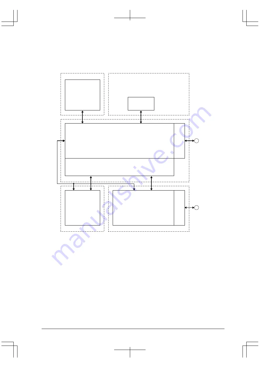
The S1C33210 consists of five major blocks: C33 Core Block, C33 Peripheral Block, C33 Analog Block, C33

DMA Block and C33 Internal Memory Block.
Figure 2.1 shows the configuration of the S1C33 blocks.

CORE_PAD

Pads

C33_SBUS

Internal RAM

(Area 0)

C33 Core Block

C33 Internal Memory Block

C33 DMA Block

PERI_PAD

Pads

C33_PERI

(Prescaler, 8-bit timer, 16-bit timer, 

Clock timer, Serial interface, 

Mobile access interface, Ports)

C33 Peripheral Block

C33 Analog Block

C33_CORE

(CPU, BCU, ITC, CLG, DBG)

C33_ADC

(A/D converter)

C33_DMA

(IDMA, HSDMA)

Figure 2.1  Block Configuration

Summary of Contents for S1C33210

Page 1: ...MF1517 01 Technical Manual CMOS 32 BIT SINGLE CHIP MICROCOMPUTER S1C33210 PRODUCT PART S1C33210 FUNCTION PART S1C33210 ...

Page 2: ...products requiring high level reliability such as medical products Moreover no license to any intellectual property rights is granted by implication or otherwise and there is no representation or warranty that anything made in accordance with this material will be free from any patent or copyright infringement of a third party This material or portions thereof may contain technology or the subject...

Page 3: ...er Starting April 1 2001 the configuration of product number descriptions will be changed as listed below To order from April 1 2001 please use these product numbers For further information please contact Epson sales representative Devices S1 C 33104 F 0A01 Packing specification Specification Package D die form F QFP Model number Model name C microcomputer digital products Product classification S...

Page 4: ......

Page 5: ...A 15 5 Power Down Control A 62 6 Basic External Wiring Diagram A 65 7 Precautions on Mounting A 66 8 Electrical Characteristics A 68 8 1 Absolute Maximum Rating A 68 8 2 Recommended Operating Conditions A 69 8 3 DC Characteristics A 70 8 4 Current Consumption A 71 8 5 A D Converter Characteristics A 72 8 6 AC Characteristics A 74 8 6 1 Symbol Description A 74 8 6 2 AC Characteristics Measurement C...

Page 6: ...PSON Appendix A Reference External Device Interface Timings A 92 A 1 DRAM 70ns A 93 A 2 DRAM 60ns A 96 A 3 ROM and Burst ROM A 100 A 4 SRAM 55ns A 102 A 5 SRAM 70ns A 104 A 6 8255A A 106 Appendix B Pin Characteristics A 107 ...

Page 7: ... Reset Pulse B II 3 2 Boot Address B II 3 3 Notes Related to Initial Reset B II 3 3 II 4 BCU BUS CONTROL UNIT B II 4 1 Pin Assignment for External System Interface B II 4 1 I O Pin List B II 4 1 Combination of System Bus Control Signals B II 4 3 Memory Area B II 4 4 Memory Map B II 4 4 External Memory Map and Chip Enable B II 4 5 Using Internal Memory on External Memory Area B II 4 7 Exclusive Sig...

Page 8: ... 5 3 Clearing Standby Mode by Interrupts B II 5 3 Trap Table B II 5 4 Control of Maskable Interrupts B II 5 5 Structure of the Interrupt Controller B II 5 5 Processor Status Register PSR B II 5 5 Interrupt Factor Flag and Interrupt Enable Register B II 5 6 Interrupt Priority Register and Interrupt Levels B II 5 8 IDMA Invocation B II 5 9 HSDMA Invocation B II 5 11 I O Memory of Interrupt Controlle...

Page 9: ...mmable Timer B III 4 1 I O Pins of 16 Bit Programmable Timers B III 4 2 Uses of 16 Bit Programmable Timers B III 4 3 Control and Operation of 16 Bit Programmable Timer B III 4 4 Controlling Clock Output B III 4 7 16 Bit Programmable Timer Interrupts and DMA B III 4 9 I O Memory of 16 Bit Programmable Timers B III 4 12 Programming Notes B III 4 25 III 5 WATCHDOG TIMER B III 5 1 Configuration of Wat...

Page 10: ...IrDA Interface B III 8 21 Setting IrDA Interface B III 8 21 Control and Operation of IrDA Interface B III 8 23 Serial Interface Interrupts and DMA B III 8 24 I O Memory of Serial Interface B III 8 28 Programming Notes B III 8 46 III 9 INPUT OUTPUT PORTS B III 9 1 Input Ports K Ports B III 9 1 Structure of Input Port B III 9 1 Input Port Pins B III 9 2 Notes on Use B III 9 2 I O Memory of Input Por...

Page 11: ...ontrol and Operation B III 10 13 HDLC Communications Mode B III 10 14 Overview B III 10 14 HDLC Communications Control and Operation B III 10 15 Mobile Access Interface Interrupts B III 10 18 Overview B III 10 18 Mobile Access Interface Interrupt Outputs B III 10 20 I O Memory for Mobile Access Interfaces B III 10 21 Important Notes on Debugging B III 10 42 ...

Page 12: ...formation B V 2 3 Setting the Registers in Dual Address Mode B V 2 3 Setting the Registers in Single Address Mode B V 2 6 Enabling Disabling DMA Transfer B V 2 7 Trigger Factor B V 2 8 Operation of HSDMA B V 2 9 Operation in Dual Address Mode B V 2 9 Operation in Single Address Mode B V 2 12 Timing Chart B V 2 13 Interrupt Function of HSDMA B V 2 15 I O Memory of HSDMA B V 2 17 Programming Notes B...

Page 13: ...S1C33210 PRODUCT PART ...

Page 14: ......

Page 15: ...atures Core CPU Seiko Epson original 32 bit RISC CPU S1C33000 built in Basic instruction set 105 instructions 16 bit fixed size Sixteen 32 bit general purpose register 32 bit ALU and 8 bit shifter Multiplication division instructions and MAC multiplication and accumulation instruction are available 20 0 ns of minimum instruction execution time at 50 MHz operation Internal memory ROM None RAM 8K by...

Page 16: ...ct interface function built in Supports fast page mode and EDO page mode Supports self refresh and CAS before RAS refresh Supports burst ROM Operating conditions and power consumption Operating voltage VDD 2 7 V to 3 6 V Operating clock frequency CPU 50 MHz max 25 MHz max Mobile access interfaces Operating temperature 40 to 85 C Power consumption During SLEEP 4 µW typ During HALT 122 mW typ 3 3 V ...

Page 17: ...SGET P31 DST 2 0 P10 12 DPCO P13 DCLK P14 T8UFx P10 13 SINx P00 P04 P27 RXD SOUTx P01 P05 P26 TXD SCLKx P02 P25 SRDYx P03 P24 P00 05 P10 16 P20 27 P30 35 DTR RTS TXD RI CTS DCD DSR RXD CNT1 CNT2 MSEL GOUT S1C33210 EXCLx P10 13 P15 P16 TMx P22 27 16 bit Programmable Timer 6 ch S1C33000 Bus Control Unit CPU Core Interrupt Controller Prescaler OSC3 PLL OSC1 Clock Timer Intelligent DMA 128 ch High spe...

Page 18: ...7 CE17 18 CE7 RAS0 CE13 RAS2 OSC2 OSC1 CE6 CE7 8 CE8 RAS1 CE14 RAS3 VSS A0 BSL A1 A2 A3 P35 BUSACK HCAS LCAS P34 BUSREQ CE6 A4 A5 No 65 66 67 68 69 70 71 72 73 74 75 76 77 78 79 80 81 82 83 84 85 86 87 88 89 90 91 92 93 94 95 96 Pin name A6 A7 VSS P30 WAIT CE4 5 A8 A9 CE5 CE15 CE15 16 A10 A20 VDD A11 A21 P16 EXCL5 DMAEND1 A12 A22 TST A13 A23 P04 SIN1 A14 A15 P05 SOUT1 A16 A17 A18 VSS A19 P20 DRD V...

Page 19: ...n CEFUNC 1 0 D A 9 0x48130 01 When CEFUNC 1 0 1x this pin outputs CE17 CE18 signal CE8 RAS1 CE14 RAS3 53 O CE8 Area 8 chip enable when CEFUNC 1 0 D A 9 0x48130 00 and A8DRA D8 0x48128 0 default RAS1 Area 8 DRAM row strobewhen CEFUNC 1 0 D A 9 0x48130 00 and A8DRA D8 0x48128 1 CE14 Area 14 chip enable when CEFUNC 1 0 D A 9 0x48130 01 or 1x and A14DRA D8 0x48122 0 RAS3 Area 14 DRAM row strobe when C...

Page 20: ...402DC 1 and IOC34 D4 0x402DE 1 P35 BUSACK 59 I O P35 I O port when CFP35 D5 0x402DC 0 default BUSACK Bus acknowledge output when CFP35 D5 0x402DC 1 P30 WAIT CE4 5 68 I O P30 I O port when CFP30 D0 0x402DC 0 default WAIT Wait cycle request input when CFP30 D0 0x402DC 1 CE4 5 Areas 4 5 chip enable when CFP30 D0 0x402DC 1 and IOC30 D0 0x402DE 1 P20 DRD 92 I O P20 I O port when CFP20 D0 0x402D8 0 defa...

Page 21: ...402DC 1 P04 SIN1 83 I O P04 I O port when CFP04 D4 0x402D0 0 and CFEX4 D4 0x402DF 0 default SIN1 Serial I F Ch 1 data input when CFP04 D4 0x402D0 1 and CFEX4 D4 0x402DF 0 P15 EXCL4 DMAEND0 128 I O P15 I O port when CFP15 D5 0x402D4 0 default EXCL4 16 bit timer 4 event counter input when CFP15 D5 0x402D4 1 and IOC15 D5 0x402D6 0 DMAEND0 HSDMA Ch 0 end of transfer signal output when CFP15 D5 0x402D4...

Page 22: ...output when CFP03 D3 0x402D0 1 P04 SIN1 83 I O P04 I O port when CFP04 D4 0x402D0 0 and CFEX4 D4 0x402DF 0 default SIN1 Serial I F Ch 1 data input when CFP04 D4 0x402D0 1 and CFEX4 D4 0x402DF 0 P05 SOUT1 86 I O P05 I O port when CFP05 D5 0x402D0 0 and CFEX5 D5 0x402DF 0 default SOUT1 Serial I FCh 1 data output when CFP05 D5 0x402D0 1 and CFEX5 D5 0x402DF 0 P10 EXCL0 T8UF0 DST0 121 I O P10 I O port...

Page 23: ... when CFP20 D0 0x402D8 0 default DRD DRAM read signal output for successive RAS mode when CFP20 D0 0x402D8 1 P21 DWE GAAS 117 I O P21 I O port when CFP21 D1 0x402D8 0 and CFEX2 D2 0x402DF 0 default DWE DRAM read signal output for successive RAS mode when CFP21 D1 0x402D8 1 and CFEX2 D2 0x402DF 0 GAAS Area address strobe for GA when CFEX2 D2 0x402DF 1 P22 TM0 118 I O P22 I O port when CFP22 D2 0x40...

Page 24: ... name Pin No I O Pull up Function QFP15 128 OSC1 51 I Low speed OSC1 oscillation input 32 kHz crystaloscillator or external clock input OSC2 50 O Low speed OSC1 oscillation output OSC3 112 I High speed OSC3 oscillation input crystal ceramicoscillator orexternal clock input OSC4 113 O High speed OSC3 oscillation output PLLS 1 0 105 106 I PLL set up pins PLLS1 PLLS0 fin fOSC3 fout fPSCIN 1 1 10 25MH...

Page 25: ...ace circuit CPU core Internal peripheral circuit VDD 2 7 to 3 6 V 2 7 to 3 6 V GND I O pins Analog circuits A D converter AVDD VSS Figure 2 1 1 Power Supply System 2 2 Operating Voltage VDD VSS The core CPU internal peripheral circuits and external signal interfaces operate on the voltage difference between the VDD and VSS pins The following operating voltage can be used VDD 2 7 V to 3 6 V VSS GND...

Page 26: ...ircuit A D converter The AVDD pin isused tosupplyan analogpower voltage and the VSS pin is used as the analog ground Supply the same voltage level as the VDD to the AVDD pin AVDD VDD VSS GND Note Be sure to supply VDD to the AVDD pin even if the analog circuit is not used Noise on the analog power lines decrease the A D converting precision so use a stabilized power supply and make the board patte...

Page 27: ...or middleware use Reserved For CPU debug mode Internal peripheral circuits Internal peripheral circuits Mirror of internal peripheral circuits Mirror of internal peripheral circuits Mirror of internal RAM Internal RAM 8KB Area Address Figure 3 1 Memory Map Area 2 is used in debug mode only and it cannot be accessed in user mode normal program execution status 3 1 ROM and Boot Address The S1C33210 ...

Page 28: ...ug Unit Functional block for debugging with the S5U1C33000H In Circuit Debugger for S1C33 Family C33 Peripheral Block Prescaler Programmable clock generator for peripheral circuits 8 bit programmable timer 6 channels with clock output function 16 bit programmable timer 6 channels with event counter clock output and watchdog timer functions Serial interface 4 channels asynchronous mode clock synchr...

Page 29: ...0 Divided clk 1 θ 1 0 Divided clk 1 θ 1 0 Divided clk 1 θ 1 0 Divided clk 8 bit timer clock select register P16TON0 P16TS02 P16TS01 P16TS00 D7 4 D3 D2 D1 D0 reserved 16 bit timer 0 clock control 16 bit timer 0 clock division ratio selection 0 0 0 0 R W R W 0 when being read θ selected by Prescaler clock select register 0x40181 16 bit timer 0 can be used as a watchdog timer 0040147 B 1 On 0 Off 1 1...

Page 30: ...3 D2 D1 D0 reserved 16 bit timer 5 clock control 16 bit timer 5 clock division ratio selection 0 0 0 0 R W R W 0 when being read θ selected by Prescaler clock select register 0x40181 004014C B 1 On 0 Off 1 1 1 1 0 0 0 0 1 1 0 0 1 1 0 0 1 0 1 0 1 0 1 0 P16TS5 2 0 Division ratio θ 4096 θ 1024 θ 256 θ 64 θ 16 θ 4 θ 2 θ 1 16 bit timer 5 clock control register 1 On 0 Off P8TON1 P8TS12 P8TS11 P8TS10 P8T...

Page 31: ...tio θ 256 θ 128 θ 64 θ 32 θ 16 θ 8 θ 4 θ 2 TCRST TCRUN D7 2 D1 D0 reserved Clock timer reset Clock timer Run Stop control X X W R W 0 when being read 0 when being read 0040151 B 1 Reset 0 Invalid 1 Run 0 Stop Clock timer Run Stop register TCISE2 TCISE1 TCISE0 TCASE2 TCASE1 TCASE0 TCIF TCAF D7 D6 D5 D4 D3 D2 D1 D0 Clock timer interrupt factor selection Clock timer alarm factor selection Interrupt f...

Page 32: ...r 0 to 65535 days high order 8 bits X X X X X X X X R W TCND15 TCND14 TCND13 TCND12 TCND11 TCND10 TCND9 TCND8 D7 D6 D5 D4 D3 D2 D1 D0 Clock timer day counter data high order 8 bits TCND15 MSB 0040158 B Clock timer day high order register 0 to 59 minutes Note Can be set within 0 63 TCCH5 TCCH4 TCCH3 TCCH2 TCCH1 TCCH0 D7 6 D5 D4 D3 D2 D1 D0 reserved Clock timer minute comparison data TCCH5 MSB TCCH0...

Page 33: ... when being read 0040164 B 1 On 0 Off 1 Preset 0 Invalid 1 Run 0 Stop 8 bit timer 1 control register 0 to 255 RLD17 RLD16 RLD15 RLD14 RLD13 RLD12 RLD11 RLD10 D7 D6 D5 D4 D3 D2 D1 D0 8 bit timer 1 reload data RLD17 MSB RLD10 LSB X X X X X X X X R W 0040165 B 8 bit timer 1 reload data register 0 to 255 PTD17 PTD16 PTD15 PTD14 PTD13 PTD12 PTD11 PTD10 D7 D6 D5 D4 D3 D2 D1 D0 8 bit timer 1 counter data...

Page 34: ... when being read 0040174 B 1 On 0 Off 1 Preset 0 Invalid 1 Run 0 Stop 8 bit timer 4 control register 0 to 255 RLD47 RLD46 RLD45 RLD44 RLD43 RLD42 RLD41 RLD40 D7 D6 D5 D4 D3 D2 D1 D0 8 bit timer 4 reload data RLD47 MSB RLD40 LSB X X X X X X X X R W 0040175 B 8 bit timer 4 reload data register 0 to 255 PTD47 PTD46 PTD45 PTD44 PTD43 PTD42 PTD41 PTD40 D7 D6 D5 D4 D3 D2 D1 D0 8 bit timer 4 counter data...

Page 35: ... Init R W Remarks WRWD D7 D6 0 EWD write protection 0 R W 0 when being read 0040170 B 1 Write enabled 0 Write protect Watchdog timer write protect register EWD D7 2 D1 D0 Watchdog timer enable 0 R W 0 when being read 0 when being read 0040171 B 1 NMI enabled 0 NMI disabled Watchdog timer enable register ...

Page 36: ...wer control register PSCDT0 D7 1 D0 reserved Prescaler clock selection 0 0 R W 0040181 B Prescaler clock select register 1 OSC1 0 OSC3 PLL HLT2OP 8T1ON PF1ON D7 4 D3 D2 D1 D0 HALT clock option OSC3 stabilize waiting function reserved OSC1 external output control 0 1 0 0 R W R W R W 0 when being read Do not write 1 0040190 B 1 On 0 Off 1 Off 0 On 1 On 0 Off Clock option register Writing 10010110 0x...

Page 37: ... 1 Error 0 Normal 1 Transmitting 0 End 1 Error 0 Normal 1 Error 0 Normal 1 Empty 0 Buffer full 1 Buffer full 0 Empty Serial I F Ch 0 status register TXEN0 RXEN0 EPR0 PMD0 STPB0 SSCK0 SMD01 SMD00 D7 D6 D5 D4 D3 D2 D1 D0 Ch 0 transmit enable Ch 0 receive enable Ch 0 parity enable Ch 0 parity mode selection Ch 0 stop bit selection Ch 0 input clock selection Ch 0 transfer mode selection 1 1 0 0 1 0 1 ...

Page 38: ...8 bit asynchronous 7 bit asynchronous 0 0 X X X X X X R W R W R W R W R W R W R W Always set to 0 Always set SMD11 to 1 00401E8 B Serial I F Ch 1 control register 1 Enabled 0 Disabled 1 Enabled 0 Disabled 1 With parity 0 No parity 1 Odd 0 Even 1 2 bits 0 1 bit 1 0 Internal clock DIVMD1 IRTL1 IRRL1 IRMD11 IRMD10 D7 5 D4 D3 D2 D1 D0 Ch 1 async clock division ratio Ch 1 IrDA I F output logic inversio...

Page 39: ...3 RXD32 RXD31 RXD30 D7 D6 D5 D4 D3 D2 D1 D0 Serial I F Ch 3 receive data RXD37 36 MSB RXD30 LSB X X X X X X X X R 00401F6 B Serial I F Ch 3 receive data register TEND3 FER3 PER3 OER3 TDBE3 RDBF3 D7 6 D5 D4 D3 D2 D1 D0 reserved Ch 3 transmit completion flag Ch 3 flaming error flag Ch 3 parity error flag Ch 3 overrun error flag Ch 3 transmit data buffer empty Ch 3 receive data buffer full 0 0 0 0 1 ...

Page 40: ... 0 0 0 0 0 R W R W R 0 when being read Always set CH2 to 0 0040242 B 1 Continuous 0 Normal A D trigger register 0 0 0 0 1 1 0 0 1 0 1 0 CE 2 0 End channel AD3 AD2 AD1 AD0 0 0 0 0 1 1 0 0 1 0 1 0 CS 2 0 Start channel AD3 AD2 AD1 AD0 CE2 CE1 CE0 CS2 CS1 CS0 D7 6 D5 D4 D3 D2 D1 D0 A D converter end channel selection A D converter start channel selection 0 0 0 0 0 0 R W R W 0 when being read Always se...

Page 41: ...being read 0040263 B High speed DMA Ch 0 1 interrupt priority register 0 to 7 0 to 7 PHSD3L2 PHSD3L1 PHSD3L0 PHSD2L2 PHSD2L1 PHSD2L0 D7 D6 D5 D4 D3 D2 D1 D0 reserved High speed DMA Ch 3 interrupt level reserved High speed DMA Ch 2 interrupt level X X X X X X R W R W 0 when being read 0 when being read 0040264 B High speed DMA Ch 2 3 interrupt priority register 0 to 7 PDM2 PDM1 PDM0 D7 3 D2 D1 D0 r...

Page 42: ...X R W R W 0 when being read 0 when being read 004026A B Serial I F Ch 1 A D interrupt priority register 0 to 7 PCTM2 PCTM1 PCTM0 D7 3 D2 D1 D0 reserved Clock timer interrupt level X X X R W Writing 1 not allowed 004026B B Clock timer interrupt priority register 0 to 7 0 to 7 PP5L2 PP5L1 PP5L0 PP4L2 PP4L1 PP4L0 D7 D6 D5 D4 D3 D2 D1 D0 reserved Port input 5 interrupt level reserved Port input 4 inte...

Page 43: ...R W R W R W 0 when being read 0 when being read 0040273 B 1 Enabled 0 Disabled 16 bit timer 2 3 interrupt enable register 1 Enabled 0 Disabled E16TC5 E16TU5 E16TC4 E16TU4 D7 D6 D5 4 D3 D2 D1 0 16 bit timer 5 comparison A 16 bit timer 5 comparison B reserved 16 bit timer 4 comparison A 16 bit timer 4 comparison B reserved 0 0 0 0 R W R W R W R W 0 when being read 0 when being read 0040274 B 1 Enabl...

Page 44: ...ead 0040283 B 1 Factor is generated 0 No factor is generated 16 bit timer 2 3 interrupt factor flag register 1 Factor is generated 0 No factor is generated F16TC5 F16TU5 F16TC4 F16TU4 D7 D6 D5 4 D3 D2 D1 0 16 bit timer 5 comparison A 16 bit timer 5 comparison B reserved 16 bit timer 4 comparison A 16 bit timer 4 comparison B reserved X X X X R W R W R W R W 0 when being read 0 when being read 0040...

Page 45: ... W 0 when being read 0040293 B 1 IDMA request 0 Interrupt request 1 IDMA request 0 Interrupt request Serial I F Ch 1 A D port input 4 7 IDMA request register DE16TC0 DE16TU0 DEHDM1 DEHDM0 DEP3 DEP2 DEP1 DEP0 D7 D6 D5 D4 D3 D2 D1 D0 16 bit timer 0 comparison A 16 bit timer 0 comparison B High speed DMA Ch 1 High speed DMA Ch 0 Port input 3 Port input 2 Port input 1 Port input 0 0 0 0 0 0 0 0 0 R W ...

Page 46: ...eed DMA Ch 2 trigger set up 0 0 0 0 0 0 0 0 R W R W 0040299 B 0 1 2 3 4 5 6 7 8 9 A B C Software trigger K54 input falling edge K54 input rising edge Port 3 input Port 7 input 8 bit timer Ch 3 underflow 16 bit timer Ch 3 compare B 16 bit timer Ch 3 compare A 16 bit timer Ch 5 compare B 16 bit timer Ch 5 compare A SI F Ch 1 Rx buffer full SI F Ch 1 Tx buffer empty A D conversion completion 0 1 2 3 ...

Page 47: ...data R R R R R 0 when being read Undefined when read 00402C1 B 1 1 High 0 0 Low K5 input port data register CP3 CP2 CP1 CP0 CFK63 CFK62 CFK61 CFK60 D7 D6 D5 D4 D3 D2 D1 D0 CP3 CP2 CP1 CP0 K63 function selection K62 function selection K61 function selection K60 function selection 0 0 0 0 0 0 0 0 R W R W R W R W R W R W R W R W Always set to 0 00402C3 B 1 0 CP3 1 0 CP2 1 0 CP1 1 0 CP0 1 AD3 0 K63 1 ...

Page 48: ...PPT4 SPPT3 SPPT2 SPPT1 SPPT0 D7 D6 D5 D4 D3 D2 D1 D0 FPT7 input polarity selection FPT6 input polarity selection FPT5 input polarity selection FPT4 input polarity selection FPT3 input polarity selection FPT2 input polarity selection FPT1 input polarity selection FPT0 input polarity selection 1 1 1 1 1 1 1 1 R W R W R W R W R W R W R W R W 00402C8 B Port input interrupt input polarity select regist...

Page 49: ...n P01 function selection P00 function selection 0 0 0 0 0 0 R W R W R W R W R W R W 0 when being read Extended functions 0x402DF 00402D0 B 1 SOUT1 0 P05 1 SIN1 0 P04 1 SRDY0 0 P03 1 SCLK0 0 P02 1 SOUT0 0 P01 1 SIN0 0 P00 P0 function select register P05D P04D P03D P02D P01D P00D D7 6 D5 D4 D3 D2 D1 D0 reserved P05 I O port data P04 I O port data P03 I O port data P02 I O port data P01 I O port data...

Page 50: ...0 R W R W R W R W R W R W R W R W 00402D9 B 1 High 0 Low P2 I O port data register IOC27 IOC26 IOC25 IOC24 IOC23 IOC22 IOC21 IOC20 D7 D6 D5 D4 D3 D2 D1 D0 P27 I O control P26 I O control P25 I O control P24 I O control P23 I O control P22 I O control P21 I O control P20 I O control 0 0 0 0 0 0 0 0 R W R W R W R W R W R W R W R W 00402DA B 1 Output 0 Input P2 I O control register SSRDY2 SSCLK2 SSOU...

Page 51: ...reas 16 15 output disable delay time reserved Areas 16 15 wait control 1 8 bits 0 16 bits 1 8 bits 0 16 bits 0 1 1 1 1 1 0 1 1 1 1 1 R W R W R W R W R W R W 0 when being read 0 when being read 0 when being read 0 when being read 0048120 HW Areas 18 15 set up register 1 1 0 0 1 0 1 0 A18DF 1 0 Number of cycles 3 5 2 5 1 5 0 5 1 1 0 0 1 0 1 0 A16DF 1 0 Number of cycles 3 5 2 5 1 5 0 5 1 1 1 1 0 0 0 ...

Page 52: ...9 device size selection Areas 10 9 output disable delay time reserved Areas 10 9 wait control 1 Used 0 Not used 1 Used 0 Not used 1 8 bits 0 16 bits 0 0 0 0 0 1 1 1 1 1 R W R W R W R W R W R W 0 when being read 0 when being read 0048126 HW 1 1 0 0 1 0 1 0 A10BW 1 0 Wait cycles 3 2 1 0 1 1 0 0 1 0 1 0 A10DF 1 0 Number of cycles 3 5 2 5 1 5 0 5 1 1 1 1 0 0 0 0 1 1 0 0 1 1 0 0 1 0 1 0 1 0 1 0 A10WT 2...

Page 53: ...4 D3 D2 D1 D0 TTBR register write protect 0 0 0 0 0 0 0 0 W Undefined in read 004812D B Writing 01011001 0x59 removes the TTBR 0x48134 write protection Writing other data sets the write protection TTBR write protect register RBCLK RBST8 REDO RCA1 RCA0 RPC2 RPC1 RPC0 RRA1 RRA0 SBUSST SEMAS SEPD SWAITE DF DE DD DC DB DA D9 D8 D7 D6 D5 D4 D3 D2 D1 D0 BCLK output control reserved Burst ROM burst mode ...

Page 54: ...Area 16 15 internal external access Area 14 13 internal external access Area 12 11 internal external access reserved Area 8 7 internal external access Area 6 internal external access Area 5 4 internal external access Area 18 17 endian control Area 16 15 endian control Area 14 13 endian control Area 12 11 endian control Area 10 9 endian control Area 8 7 endian control Area 6 endian control Area 5 4...

Page 55: ... 4 address strobe signal Area 18 17 read signal Area 16 15 read signal Area 14 13 read signal Area 12 11 read signal reserved Area 8 7 read signal Area 6 read signal Area 5 4 read signal 0 0 0 0 0 0 0 0 0 0 0 0 0 0 0 0 R W R W R W R W R W R W R W R W R W R W R W R W R W R W 0 when being read 0 when being read 0048138 HW G A read signal control register 1 Enabled 0 Disabled 1 Enabled 0 Disabled A1X...

Page 56: ...2 HW 16 bit timer 0 comparison register B 0 to 65535 TC015 TC014 TC013 TC012 TC011 TC010 TC09 TC08 TC07 TC06 TC05 TC04 TC03 TC02 TC01 TC00 DF DE DD DC DB DA D9 D8 D7 D6 D5 D4 D3 D2 D1 D0 16 bit timer 0 counter data TC015 MSB TC00 LSB X X X X X X X X X X X X X X X X R 0048184 HW 16 bit timer 0 counter data register SELFM0 SELCRB0 OUTINV0 CKSL0 PTM0 PRESET0 PRUN0 D7 D6 D5 D4 D3 D2 D1 D0 reserved 16 ...

Page 57: ...A HW 16 bit timer 1 comparison register B 0 to 65535 TC115 TC114 TC113 TC112 TC111 TC110 TC19 TC18 TC17 TC16 TC15 TC14 TC13 TC12 TC11 TC10 DF DE DD DC DB DA D9 D8 D7 D6 D5 D4 D3 D2 D1 D0 16 bit timer 1 counter data TC115 MSB TC10 LSB X X X X X X X X X X X X X X X X R 004818C HW 16 bit timer 1 counter data register SELFM1 SELCRB1 OUTINV1 CKSL1 PTM1 PRESET1 PRUN1 D7 D6 D5 D4 D3 D2 D1 D0 reserved 16 ...

Page 58: ...2 HW 16 bit timer 2 comparison register B 0 to 65535 TC215 TC214 TC213 TC212 TC211 TC210 TC29 TC28 TC27 TC26 TC25 TC24 TC23 TC22 TC21 TC20 DF DE DD DC DB DA D9 D8 D7 D6 D5 D4 D3 D2 D1 D0 16 bit timer 2 counter data TC215 MSB TC20 LSB X X X X X X X X X X X X X X X X R 0048194 HW 16 bit timer 2 counter data register SELFM2 SELCRB2 OUTINV2 CKSL2 PTM2 PRESET2 PRUN2 D7 D6 D5 D4 D3 D2 D1 D0 reserved 16 ...

Page 59: ...A HW 16 bit timer 3 comparison register B 0 to 65535 TC315 TC314 TC313 TC312 TC311 TC310 TC39 TC38 TC37 TC36 TC35 TC34 TC33 TC32 TC31 TC30 DF DE DD DC DB DA D9 D8 D7 D6 D5 D4 D3 D2 D1 D0 16 bit timer 3 counter data TC315 MSB TC30 LSB X X X X X X X X X X X X X X X X R 004819C HW 16 bit timer 3 counter data register SELFM3 SELCRB3 OUTINV3 CKSL3 PTM3 PRESET3 PRUN3 D7 D6 D5 D4 D3 D2 D1 D0 reserved 16 ...

Page 60: ...2 HW 16 bit timer 4 comparison register B 0 to 65535 TC415 TC414 TC413 TC412 TC411 TC410 TC49 TC48 TC47 TC46 TC45 TC44 TC43 TC42 TC41 TC40 DF DE DD DC DB DA D9 D8 D7 D6 D5 D4 D3 D2 D1 D0 16 bit timer 4 counter data TC415 MSB TC40 LSB X X X X X X X X X X X X X X X X R 00481A4 HW 16 bit timer 4 counter data register SELFM4 SELCRB4 OUTINV4 CKSL4 PTM4 PRESET4 PRUN4 D7 D6 D5 D4 D3 D2 D1 D0 reserved 16 ...

Page 61: ...A HW 16 bit timer 5 comparison register B 0 to 65535 TC515 TC514 TC513 TC512 TC511 TC510 TC59 TC58 TC57 TC56 TC55 TC54 TC53 TC52 TC51 TC50 DF DE DD DC DB DA D9 D8 D7 D6 D5 D4 D3 D2 D1 D0 16 bit timer 5 counter data TC515 MSB TC50 LSB X X X X X X X X X X X X X X X X R 00481AC HW 16 bit timer 5 counter data register SELFM5 SELCRB5 OUTINV5 CKSL5 PTM5 PRESET5 PRUN5 D7 D6 D5 D4 D3 D2 D1 D0 reserved 16 ...

Page 62: ...1 0 0 0 0 0 R W 0048200 HW IDMA base address low order register DBASEH11 DBASEH10 DBASEH9 DBASEH8 DBASEH7 DBASEH6 DBASEH5 DBASEH4 DBASEH3 DBASEH2 DBASEH1 DBASEH0 DF C DB DA D9 D8 D7 D6 D5 D4 D3 D2 D1 D0 reserved IDMA base address high order 12 bits Initial value 0x0C003A0 0 0 0 0 1 1 0 0 0 0 0 0 R W Undefined in read 0048202 HW IDMA base address high order register 0 to 127 DSTART DCHN D7 D6 0 IDM...

Page 63: ...y WR 0 Memory RD 0 0 X X X X X X X X R W R W R W Undefined in read 0048222 HW High speed DMA Ch 0 control register Note D Dual address mode S Single address mode S0ADRL15 S0ADRL14 S0ADRL13 S0ADRL12 S0ADRL11 S0ADRL10 S0ADRL9 S0ADRL8 S0ADRL7 S0ADRL6 S0ADRL5 S0ADRL4 S0ADRL3 S0ADRL2 S0ADRL1 S0ADRL0 DF DE DD DC DB DA D9 A8 D7 D6 D5 D4 D3 D2 D1 D0 D Ch 0 source address 15 0 S Ch 0 memory address 15 0 X ...

Page 64: ...RH2 D0ADRH1 D0ADRH0 DF DE DD DC DB DA D9 A8 D7 D6 D5 D4 D3 D2 D1 D0 Ch 0 transfer mode D Ch 0 destination address control S Invalid D Ch 0 destination address 27 16 S Invalid 0 0 0 0 X X X X X X X X X X X X R W R W R W 004822A HW High speed DMA Ch 0 high order destination address set up register Note D Dual address mode S Single address mode 1 1 0 0 1 0 1 0 D0MOD 1 0 Mode Invalid Block Successive ...

Page 65: ...y WR 0 Memory RD 0 0 X X X X X X X X R W R W R W Undefined in read 0048232 HW High speed DMA Ch 1 control register Note D Dual address mode S Single address mode S1ADRL15 S1ADRL14 S1ADRL13 S1ADRL12 S1ADRL11 S1ADRL10 S1ADRL9 S1ADRL8 S1ADRL7 S1ADRL6 S1ADRL5 S1ADRL4 S1ADRL3 S1ADRL2 S1ADRL1 S1ADRL0 DF DE DD DC DB DA D9 A8 D7 D6 D5 D4 D3 D2 D1 D0 D Ch 1 source address 15 0 S Ch 1 memory address 15 0 X ...

Page 66: ...RH2 D1ADRH1 D1ADRH0 DF DE DD DC DB DA D9 A8 D7 D6 D5 D4 D3 D2 D1 D0 Ch 1 transfer mode D Ch 1 destination address control S Invalid D Ch 1 destination address 27 16 S Invalid 0 0 0 0 X X X X X X X X X X X X R W R W R W 004823A HW High speed DMA Ch 1 high order destination address set up register Note D Dual address mode S Single address mode 1 1 0 0 1 0 1 0 D1MOD 1 0 Mode Invalid Block Successive ...

Page 67: ...y WR 0 Memory RD 0 0 X X X X X X X X R W R W R W Undefined in read 0048242 HW High speed DMA Ch 2 control register Note D Dual address mode S Single address mode S2ADRL15 S2ADRL14 S2ADRL13 S2ADRL12 S2ADRL11 S2ADRL10 S2ADRL9 S2ADRL8 S2ADRL7 S2ADRL6 S2ADRL5 S2ADRL4 S2ADRL3 S2ADRL2 S2ADRL1 S2ADRL0 DF DE DD DC DB DA D9 A8 D7 D6 D5 D4 D3 D2 D1 D0 D Ch 2 source address 15 0 S Ch 2 memory address 15 0 X ...

Page 68: ...RH2 D2ADRH1 D2ADRH0 DF DE DD DC DB DA D9 A8 D7 D6 D5 D4 D3 D2 D1 D0 Ch 2 transfer mode D Ch 2 destination address control S Invalid D Ch 2 destination address 27 16 S Invalid 0 0 0 0 X X X X X X X X X X X X R W R W R W 004824A HW High speed DMA Ch 2 high order destination address set up register Note D Dual address mode S Single address mode 1 1 0 0 1 0 1 0 D2MOD 1 0 Mode Invalid Block Successive ...

Page 69: ...y WR 0 Memory RD 0 0 X X X X X X X X R W R W R W Undefined in read 0048252 HW High speed DMA Ch 3 control register Note D Dual address mode S Single address mode S3ADRL15 S3ADRL14 S3ADRL13 S3ADRL12 S3ADRL11 S3ADRL10 S3ADRL9 S3ADRL8 S3ADRL7 S3ADRL6 S3ADRL5 S3ADRL4 S3ADRL3 S3ADRL2 S3ADRL1 S3ADRL0 DF DE DD DC DB DA D9 A8 D7 D6 D5 D4 D3 D2 D1 D0 D Ch 3 source address 15 0 S Ch 3 memory address 15 0 X ...

Page 70: ...RH2 D3ADRH1 D3ADRH0 DF DE DD DC DB DA D9 A8 D7 D6 D5 D4 D3 D2 D1 D0 Ch 3 transfer mode D Ch 3 destination address control S Invalid D Ch 3 destination address 27 16 S Invalid 0 0 0 0 X X X X X X X X X X X X R W R W R W 004825A HW High speed DMA Ch 3 high order destination address set up register Note D Dual address mode S Single address mode 1 1 0 0 1 0 1 0 D3MOD 1 0 Mode Invalid Block Successive ...

Page 71: ...eed switch for data conversion Frame frequency division switch 0 0 0 R W R W R W 0 when being read 0200010 HW 1 Convert 0 Pass through 1 32kbps 0 64kbps 1 Frequency divider 0 Pass through Communications block PHS mode settings register CP0EN4 CP0EN3 CP0EN2 CP0EN1 CP0EN0 D15 5 D4 D3 D2 D1 D0 Assign UINT4 to CP0 Assign UINT3 to CP0 Assign UINT2 to CP0 Assign UINT1 to CP0 Assign UINT0 to CP0 0 0 0 0 ...

Page 72: ...e 1 Enable 0 Disable Communications block modem status interrupt enable register DTR RTS D15 2 D1 D0 DTR output level RTS output level 0 0 R W R W 0 when being read Only valid for UART operation 020002E HW 1 DTR H 0 DTR L 1 RTS H 0 RTS L Communications block modem control register STOP D15 1 D0 Debugging HOLD input control 0 R W 0 when being read 0200032 HW 1 HOLD input 0 No input Communications b...

Page 73: ...etting HDLC enable transmit setting HDLC enable receive interrupt setting HDLC enable transmit interrupt setting 0 0 0 0 R W R W R W R W 0 when being read Writes of 0 are ignored Writes of 0 are ignored 0 when being read Writes of 0 are ignored Writes of 0 are ignored 0200308 HW 1 Enable 0 Disable 1 Enable 0 Disable 1 Enable 0 Disabled 1 Enable 0 Disabled HDLC transfer settings register RXENC TXEN...

Page 74: ... RTXU D15 8 D7 D6 D5 D4 1 D0 HDLC reset TXUDR EOM latch HDLC transmit abort setting HDLC transmit queue reset HDLC reset TXUDR flag 0 0 0 0 W W W W 0 when being read Writes of 0 are ignored Writes of 0 are ignored Writes of 0 are ignored 0 when being read Writes of 0 are ignored 020031C HW 1 Reset latch 0 Ignored 1 Transmit abort pattern 0 Ignored 1 Reset queue 0 Ignored 1 Reset flag 0 Ignored HDL...

Page 75: ... RESID 1 0200332 HW HDLC residue code register TXUE TXBRDY TXUDR D15 8 D7 D6 D5 1 D0 Tx underrun EOM detected Transmit queue not full Transmit queue underrun X X X R R R 0 when being read 0 when being read 0200334 HW HDLC transmit status register 1 not Full 0 Full 1 Yes 0 No 1 Under run 0 No underrun ESINT SPINT RXINT TXINT D15 8 D7 D6 D5 D4 D3 0 E S INT interrupt Sp INT interrupt Rx INT interrupt...

Page 76: ...nal is asserted from an external bus master while SEPD D1 Bus control register 0x4812E 1 CPU and DMA HALT2 mode Execute the halt instruction after setting HLT2OP to 1 CPU BCU bus clock and DMA SLEEP mode Execute the slp instruction CPU BCU bus clock DMA high speed OSC3 oscillation circuit prescaler and peripheral circuits that use the prescaler output clocks HLT2OP D3 Clock option register 0x40190...

Page 77: ... 4 01 1 2 00 1 1 1 1 Turning off the prescaler and peripheral circuits Current consumption can be reduced by turning off the peripheral circuits operating at high speed as much as possible This applies to the following peripheral circuits 1 Blocks that use an operating clock generated by the prescaler 16 bit programmable timers 0 to 5 watchdog timer 8 bit programmable timers 0 to 5 DRAM refresh se...

Page 78: ... 8 bit timer 0 1 clock control register 0x4014D ON OFF OFF 8 bit timer 1 Run Stop PTRUN1 D0 8 bit timer 1 control register 0x40164 RUN STOP STOP 8 bit timer 2 clock control P8TON2 D3 8 bit timer 2 3 clock control register 0x4014E ON OFF OFF 8 bit timer 2 Run Stop PTRUN2 D0 8 bit timer 2 control register 0x40168 RUN STOP STOP 8 bit timer 3 clock control P8TON3 D7 8 bit timer 2 3 clock control regis...

Page 79: ...potential of the substrate back of the chip is VSS CG2 C2 C1 R1 1 HSDMA Mobile access Interface input Mobile access Interface output CD1 X tal1 Rf1 CG1 X tal1 CG1 CD1 Rf1 X tal2 CR CG2 CD2 Rf2 R1 C1 C2 Crystal oscillator Gate capacitor Drain capacitor Feedback resistor Crystal oscillator Ceramic oscillator Gate capacitor Drain capacitor Feedback resistor Resistor Capacitor Capacitor 32 768 kHz CI ...

Page 80: ...SS Sample VSS pattern OSC3 and OSC4 VSS PLLC VSS PLLC 3 When supplying an external clock to the OSC3 OSC1 pin the clock source should be connected to the OSC3 OSC1 pin in the shortest line Furthermore do not connect anything else to the OSC4 OSC2 pin In order to prevent unstable operation of the oscillation circuit due to current leak between OSC3 OSC1 and VDD please keep enough distance between O...

Page 81: ...noise caused by mutual inductance do not arrange a large current signal line near the circuits that are sensitive to noise such as theoscillation unitandanaloginput unit When a signal line is parallel with a high speed line in long distance or intersects a high speed line noise may generated by mutual interference between the signals and it may cause a malfunction Do not arrange a high speed signa...

Page 82: ...dition Rated value Unit Supply voltage VDD 0 3 to 4 0 V Input voltage VI 0 3 to VDDE 0 5 V High level output current IOH 1 pin 10 mA Total of all pins 40 mA Low level output current IOL 1 pin 10 mA Total of all pins 40 mA Analog power voltage AVDDE 0 3 to 7 0 V Analog input voltage AVIN 0 3 to AVDDE 0 3 V Storage temperature TSTG 65 to 150 C ...

Page 83: ...it Supply voltage VDD 2 70 3 60 V Input voltage VI VSS VDD V CPU operating clock frequency fCPU 50 MHz Low speed oscillation frequency fOSC1 32 768 kHz Operating temperature Ta 40 25 85 C Input rise time normal input tri 50 ns Input fall time normal input tfi 50 ns Input rise time schmitt input tri 5 ms Input fall time schmitt input tfi 5 ms ...

Page 84: ...pe2 IOL 12mA Type3 VDD Min 0 4 V High level input voltage VIH CMOS level VDD Max 2 4 V Low level input voltage VIL CMOS level VDD Min 0 4 V Positive trigger input voltage VT LVTTL schmitt 1 1 2 4 V Negative trigger input voltage VT LVTTL schmitt 0 6 1 8 V Hysteresis voltage VH LVTTL schmitt 0 1 V Pull up resistor RPU VI 0V Other than DSIO 80 200 480 kΩ DSIO 40 100 240 kΩ Pull down resistor RPD VI ...

Page 85: ...o 85 C Item Symbol Condition Min Typ Max Unit A D converter operating current AIDD1 VDD AVDD 2 7V to 3 6V 500 800 µA 6 Current consumption measurement condition VIH VDD VIL 0V output pins are open note No OSC3 OSC1 CPU Clock timer Other peripheral circuits 1 On Off Normal operation 1 Stop Stop 2 On Off HALT mode Stop Stop 3 On Off HALT2 mode Stop Stop 4 Off Off SLEEP mode Stop Stop 5 Off On HALT m...

Page 86: ...uency in 3V system Note Be sure to use as VDD AVDD The A D converter cannot be used when the S1C33210 is used with a 2V power source A D conversion error V 000 h Ideal voltage at zero scale point 0 5LSB V 000 h Actual voltage at zero scale point V 3FF h Ideal voltage at full scale point 1022 5LSB V 3FF h Actual voltage at full scale point 1LSB 1LSB AVDD VSS 210 1 V 3FF h V 000 h 210 2 V 000 h 0 5L...

Page 87: ...SB Digital output hex Analog input Ideal conversion characteristic Actual conversion characteristic V 3FF h V N h VN VN V N 1 h N 1 N N 1 N 2 Integral linearity error Differential linearity error Differential linearity error ED 1 LSB V N h V N 1 h 1LSB Digital output hex Analog input Ideal conversion characteristic Actual conversion characteristic ...

Page 88: ...ite cycle is actually extended when 2 or more wait cycles are set When inserting wait cycles by controlling the WAIT pin from outside of the IC pay attention to thetiming of the WAIT signal sampling Read cycles are terminated at the cycle in which the WAIT signal is negated Write cycles are terminated at the following cycle after the WAIT signal is negated C1 C2 C3 Cn Cycle number C1 indicates the...

Page 89: ...bol Min Max Unit High speed clock cycle time tC3 30 ns OSC3 clock input duty tC3ED 45 55 OSC3 clock input rise time tIF 5 ns OSC3 clock input fall time tIR 5 ns BCLK high level output delay time tCD1 35 ns BCLK low level output delay time tCD2 35 ns Minimum reset pulse width tRST 6 tCYC ns BCLK clock output characteristics Note These AC characteristic values are applied only when the high speed os...

Page 90: ... time 2 tWDD2 0 10 ns Write data hold time tWDH 0 ns note 1 This applies to the BSH and BSL timings 2 This applies to the GAAS and GARD timings 3 This applies to the GAAS timing SRAM read cycle Unless otherwise specified VDD 2 7V to 3 6V VSS 0V Ta 40 C to 85 C Item Symbol Min Max Unit Read signal delay time 2 tRDD2 10 ns Read signal pulse width tRDW tCYC 0 5 WC 10 ns Read address access time 1 tAC...

Page 91: ...6V VSS 0V Ta 40 C to 85 C Item Symbol Min Max Unit Column address access time tACCE tCYC 1 5 WC 25 ns RAS access time tRACE tCYC 2 WC 25 ns CAS access time tCACE tCYC 1 WC 20 ns Read data setup time tRDS2 20 ns Burst ROM read cycle Unless otherwise specified VDD 2 7V to 3 6V VSS 0V Ta 40 C to 85 C Item Symbol Min Max Unit Read address access time 2 tACC2 tCYC 1 WC 25 ns Chip enable access time 2 t...

Page 92: ...aracteristic Timing Charts Clock OSC3 High speed clock tC3 BCLK Clock output tC3 tC3H tC3ED tC3H tC3 tCBD tCBH tC3 BCLK Clock output tC3 tCBH tCD1 tCD2 tIF tIR 1 When an external clock is input in x1 speed mode 2 When the high speed oscillation circuit is used for the operating clock ...

Page 93: ... measured with respect to the first signal change negation from among the RD CEx and A 23 0 signals SRAM read cycle when a wait cycle is inserted BCLK A 23 0 CEx RD D 15 0 WAIT C1 Cw wait cycle Cn last cycle tAD tCE1 tCE2 tRDD2 tRDD1 C1 only tRDAC1 tRDS tWTS tWTH tWTS tWTH tRDH tCEAC1 tACC1 tRDW tAD 1 tWTS tWTH 1 tRDH is measured with respect to the first signal change negation from among the RD C...

Page 94: ...x WR D 15 0 WAIT C1 C2 tAD tCE1 tCE2 tWRD2 tWRD1 tWTS tWTH tWDD1 tWDH tWRW tAD SRAM write cycle when wait cycles are inserted BCLK A 23 0 CEx WR D 15 0 WAIT C1 Cw wait cycle Cw wait cycle Cn last cycle tAD tCE1 tCE2 tWRD2 tWRD1 tWTS tWTH tWTS tWTS tWTH tWTH tWDD1 tWDH tWRW tAD Wait cycle follows Last cycle follows ...

Page 95: ...W tCACF 1 1 tRDH is measured with respect to the first signal change negation of either the RD or theA 23 0 signals DRAM fast page access cycle BCLK A 23 0 RAS HCAS LCAS RD D 15 0 WE D 15 0 RAS1 Data transfer 1 Data transfer 2 Next data transfer CAS1 CAS2 PRE1 precharge RAS1 tAD tAD tAD tRDS tACCF tRACF tRDH tRASD2 tRASD1 tRDD3 tRDD1 tWRD3 tWRD1 tWDD1 tWDD2 tWDD2 tCACF tACCF tRASW tRDW2 tCASD2 tCA...

Page 96: ...tCACE 1 1 tRDH is measured with respect to the first signal change negation of either the RD or the RASx signals EDO DRAM page access cycle BCLK A 23 0 RAS HCAS LCAS RD D 15 0 WE D 15 0 RAS1 Data transfer 1 Data transfer 2 Next data transfer CAS1 CAS2 PRE1 precharge RAS1 tAD tAD tAD tRDS tACCE tRACE tRASD2 tRASD1 tRDD3 tRDD1 tWRD3 tWRD1 tWDD1 tWDD2 tWDD2 tCACE tACCE tRASW tRDW2 tCASD2 tCASD1 tCASW...

Page 97: ...tup Self refresh mode tCASD2 Self refresh mode canceration tRASD2 tRASD1 tCASD1 6 cycle precharge Fixed Burst ROM read cycle BCLK A 23 2 A 1 0 CEx RD D 15 0 SRAM read cycle Burst cycle Burst cycle Burst cycle tAD tAD tAD tRDS tRDAC2 tCEAC tRDH tCE2 tCE1 tRDD2 tRDD1 tAD tAD tAD tAD tACC2 tRDS tRDH tACCB tRDS tRDH tACCB tRDS tRDH tACCB 1 1 tRDH is measured with respect to the first signal change neg...

Page 98: ...UT signals 1 eBUS_OUT signals 1 NMI tBRQS Valid input tNMIW tBRQH tBAKD tZ2E tB2Z 1 eBUS_OUT indicates the following pins A 23 0 RD WRL WRH HCAS LCAS CE 17 4 D 15 0 Input output and I O port timing BCLK Kxx Pxx input data read from the port Pxx Rxx output Kxx K port interrupt input tINPS Valid input tKINW tINPH tOUTD ...

Page 99: ...quency power voltage deviation f V 10 10 ppm V Frequency adjustment range f CG CG CD1 5 to 25pF 50 ppm 1 Q11C02RX Crystal resonator made by Seiko Epson 2 CG1 CD1 15pF includes board capacitance OSC3 crystal oscillation Note A crystal resonator that uses a fundamental should be used for the OSC3 crystal oscillation circuit Unless otherwise specified VSS 0V crystal Q22MA306 1 33 8688MHz Rf2 1MΩ CG1 ...

Page 100: ...de Fin OSC3 clock Fout 1 1 x2 10 to 25MHz 20 to 50MHz 0 1 x4 10 to 12 5MHz 40 to 50MHz 0 0 PLL not used PLL characteristics Unless otherwise specified VDD 2 7V to 3 6V VSS 0V crystal oscillator Q3204DC 1 R1 4 7kΩ C1 100pF C2 5pF Ta 40 C to 85 C Item Symbol Condition Min Typ Max Unit Jitter peak jitter tpj 1 1 ns Lockup time tpll 1 ms 1 Q3204DC Crystal oscillator made by Seiko Epson ...

Page 101: ...culated from environment temperature Ta thermal package resistance θ and power consumption PD Chip temperature Tj Ta PD θ C As a guide normally keep the chip temperature Tj lower than 85 C The thermal resistance of the QFP15 128pin package is as follows Thermal resistance C W 110 to 120 C 90 to 100 C for Cu lead frame This thermal resistance is a value under the condition that the measured device ...

Page 102: ...C33210 PRODUCT PART 10 Pad Layout 10 1 Pad Layout Diagram X Y 0 0 TBD mm TBD mm 1 5 10 15 20 25 30 35 40 45 50 55 60 65 70 75 80 85 90 95 100 105 110 115 120 125 130 135 140 145 150 155 160 165 170 175 180 185 190 195 200 Die No ...

Page 103: ...966 22 N C 0 588 2 54 72 D2 2 834 0 882 23 D13 0 504 2 54 73 N C 2 834 0 798 24 N C 0 42 2 54 74 RESET 2 834 0 714 25 P32 DMAACK0 0 336 2 54 75 N C 2 834 0 63 26 D12 0 252 2 54 76 NMI 2 834 0 546 27 P33 DMAACK1 0 168 2 54 77 N C 2 834 0 462 28 D11 0 084 2 54 78 D1 2 834 0 378 29 P02 SCLK0 0 2 54 79 N C 2 834 0 294 30 D10 0 084 2 54 80 D0 2 834 0 21 31 K50 DMAREQ0 0 168 2 54 81 VDD 2 834 0 126 32 W...

Page 104: ...PLLC 2 834 1 47 123 N C 1 092 2 54 173 N C 2 834 1 386 124 A20 1 008 2 54 174 N C 2 834 1 302 125 N C 0 924 2 54 175 VSS 2 834 1 218 126 VDD 0 84 2 54 176 N C 2 834 1 134 127 N C 0 756 2 54 177 PLLS1 2 834 1 05 128 A11 0 672 2 54 178 N C 2 834 0 966 129 N C 0 588 2 54 179 PLLS0 2 834 0 882 130 A21 0 504 2 54 180 N C 2 834 0 798 131 N C 0 42 2 54 181 RXD SIN3 2 834 0 714 132 P16 EXCL5 DMAEND1 0 336...

Page 105: ...L3 T8UF3 DPC0 2 834 1 722 211 P14 FOSC1 DCLK 2 834 1 806 212 P24 TM2 SRDY2 2 834 1 89 213 N C 2 834 1 974 214 P25 TM3 SCLK2 2 834 2 058 215 N C 2 834 2 154 216 N C 2 834 2 154 Note The S1C33210 is constructed with 0 35 µm process technology Since the pad pitch is to small it is impossible to use all pads when mounting the chip die form on the board When mounting the chip use the pads other than N ...

Page 106: ...r of cycles should be determined by referring the manual or specification of the device to be used It is necessary to set the timing values allowing ample margin according to the load capacitance of the bus and signal lines number of devices to be connected operating temperature range I O levels and other conditions The number of cycles described in this section is an example and the conditions ar...

Page 107: ...0 5 25 Column address setup time tASC 0 0 5 15 0 5 20 0 5 25 RAS CAS delay time tRCD 20 2 0 60 1 0 40 1 0 50 RAS column address delay time tRAD 15 1 5 45 0 5 20 0 5 25 Read cycle parameters RAS access time tRAC 70 4 5 135 2 5 100 2 5 125 CAS access time tCAC 20 2 5 75 1 5 60 1 5 75 Address access time tAA 35 3 0 90 2 0 80 2 0 100 OE access time tOAC 20 4 5 135 2 5 100 2 5 125 Output buffer turn of...

Page 108: ...BCLK A 11 0 RAS CAS RD D 15 0 RD WE D 15 0 WR ROW 1 RD data ROW 2 tDH tDS WR data COL 1 DRAM 70ns CPU 33MHz page mode read write cycle 2 RAS cycle CAS cycle RAS precharge 3 CAS cycle 3 tPC tACP tCP tRAS 2 BCLK A 11 0 RAS CAS RD D 15 0 RD WE D 15 0 WR ROW 1 RD data RD data WR data WR data COL 1 COL 2 DRAM 70ns CPU 33MHz CAS before RAS refresh cycle 1 1 RPC delay Fixed Refresh RAS pulse width 3 RAS ...

Page 109: ... 15 0 RD WE D 15 0 WR ROW 1 RD data ROW 2 WR data COL 1 DRAM 70ns CPU 25 20MHz page mode read write cycle 1 RAS cycle CAS cycle RAS precharge 2 CAS cycle 2 2 tRAS BCLK A 11 0 RAS CAS RD D 15 0 RD WE D 15 0 WR ROW 1 RD data RD data WR data WR data COL 1 COL 2 DRAM 70ns CPU 25 20MHz CAS before RAS refresh cycle 1 1 RPC delay Fixed Refresh RAS pulse width 2 RAS precharge 2 tRPC tCSR tCHR tRAS BCLK RA...

Page 110: ...0 5 25 Column address setup time tASC 0 0 5 15 0 5 20 0 5 25 RAS CAS delay time tRCD 20 2 0 60 1 0 40 1 0 50 RAS column address delay time tRAD 15 1 5 45 0 5 20 0 5 25 Read cycle parameters RAS access time tRAC 60 3 5 105 2 5 100 2 5 125 CAS access time tCAC 15 1 5 45 1 5 60 1 5 75 Address access time tAA 30 2 0 60 2 0 80 2 0 100 OE access time tOAC 15 3 5 105 2 5 100 2 5 125 Output buffer turn of...

Page 111: ...BCLK A 11 0 RAS CAS RD D 15 0 RD WE D 15 0 WR ROW 1 RD data ROW 2 tDH tDS WR data COL 1 DRAM 60ns CPU 33MHz page mode read write cycle 2 RAS cycle CAS cycle RAS precharge 2 CAS cycle 2 tPC tACP tCP tRAS 2 BCLK A 11 0 RAS CAS RD D 15 0 RD WE D 15 0 WR ROW 1 RD data RD data WR data WR data COL 1 COL 2 DRAM 60ns CPU 33MHz CAS before RAS refresh cycle 1 1 RPC delay Fixed Refresh RAS pulse width 3 RAS ...

Page 112: ... D 15 0 RD WE D 15 0 WR ROW 1 RD data ROW 2 WR data COL 1 DRAM 60ns CPU 25MHz page mode read write cycle 1 RAS cycle CAS cycle RAS precharge 2 CAS cycle 2 2 tRAS BCLK A 11 0 RAS CAS RD D 15 0 RD WE D 15 0 WR ROW 1 RD data RD data WR data WR data COL 1 COL 2 DRAM 60ns CPU 25MHz CAS before RAS refresh cycle 1 1 RPC delay Fixed Refresh RAS pulse width 2 RAS precharge 2 tRPC tCSR tCHR tRAS BCLK RAS CA...

Page 113: ... D 15 0 RD WE D 15 0 WR ROW 1 RD data ROW 2 WR data COL 1 DRAM 60ns CPU 20MHz page mode read write cycle 1 RAS cycle CAS cycle RAS precharge 2 CAS cycle 2 1 tRAS BCLK A 11 0 RAS CAS RD D 15 0 RD WE D 15 0 WR ROW 1 RD data RD data WR data WR data COL 1 COL 2 DRAM 60ns CPU 20MHz CAS before RAS refresh cycle 1 1 RPC delay Fixed Refresh RAS pulse width 2 RAS precharge 1 tRPC tCSR tCHR tRAS BCLK RAS CA...

Page 114: ...g Burst ROM and mask ROM interface 33MHz 25MHz 20MHz Parameter Symbol Min Max Cycle Time Cycle Time Cycle Time Access time tACC 100 5 150 4 160 3 150 CE output delay time tCE 100 5 150 4 160 3 150 OE output delay time tOE 50 4 5 135 3 5 140 2 5 125 Burst access time tBAC 50 3 90 2 80 2 100 Output disable delay time tDF 0 40 1 5 45 1 5 60 1 5 75 ROM 100ns CPU 33MHz normal read tACC tCE tOE BCLK A 2...

Page 115: ... RD D 15 0 RD data ROM 100ns CPU 25MHz burst read Normal read cycle Burst read cycle BCLK A 23 0 CE9 10 RD D 15 0 RD data RD data RD data RD data ROM 100ns CPU 20MHz normal read BCLK A 23 0 CE9 10 RD D 15 0 RD data ROM 100ns CPU 20MHz burst read Normal read cycle Burst read cycle BCLK A 23 0 CE9 10 RD D 15 0 RD data RD data RD data RD data ...

Page 116: ...tRC 55 3 90 3 120 2 100 Address access time tACC 55 3 90 3 120 2 100 CE access time tACS 55 3 90 3 120 2 100 OE access time tOE 30 2 5 75 2 5 100 1 5 75 Output disable delay time tOHZ 0 30 1 5 45 1 5 60 1 5 75 Write cycle Write cycle time tWC 55 3 90 3 120 2 100 Address enable time tAW 50 2 5 75 2 5 100 1 5 75 Write pulse width tWP 45 2 60 2 80 1 50 Input data setup time tDW 30 2 60 2 80 1 50 Inpu...

Page 117: ...A REFERENCE EXTERNAL DEVICE INTERFACE TIMINGS S1C33210 PRODUCT PART EPSON A 103 SRAM 55ns CPU 20MHz read cycle BCLK A 23 0 CEx RD D 15 0 RD data SRAM 55ns CPU 20MHz write cycle BCLK A 23 0 CEx WP D 15 0 WR data ...

Page 118: ...C 70 4 120 3 120 3 150 Address access time tACC 70 4 120 3 120 3 150 CE access time tACS 70 4 120 3 120 3 150 OE access time tOE 40 3 5 105 2 5 100 2 5 125 Output disable delay time tOHZ 0 30 1 5 45 1 5 60 1 5 75 Write cycle Write cycle time tWC 70 4 120 3 120 3 150 Address enable time tAW 60 3 5 105 2 5 100 2 5 125 Write pulse width tWP 55 3 90 2 80 2 100 Input data setup time tDW 30 3 90 2 80 2 ...

Page 119: ...EFERENCE EXTERNAL DEVICE INTERFACE TIMINGS S1C33210 PRODUCT PART EPSON A 105 SRAM 70ns CPU 25 20MHz read cycle BCLK A 23 0 CEx RD D 15 0 RD data SRAM 70ns CPU 25 20MHz write cycle BCLK A 23 0 CEx WP D 15 0 WR data ...

Page 120: ... 14 420 11 440 9 450 Input data setup time tDW 100 14 420 11 440 9 450 Input data hold time 3 tDH 30 0 5 15 0 5 20 0 5 25 1 The S1C33210 enables up to 7 cycles of wait cycle insertion If a number of wait cycles more than 7 cycles needs to be inserted input the WAIT signal from external hardware Note that the interface must be set for SRAM type devices to insert wait cycles using the WAIT pin Refer...

Page 121: ...VTTL 2 mA VDD 19 K50 DMAREQ0 XIBHP2 CMOS LVTTL SCHMITT 2 mA Pull up VDD 20 WRL WR WE XBB1 Note 2 2 mA VDD 21 WRH BSH XBB1 Note 2 2 mA VDD 22 VSS 23 K51 DMAREQ1 XIBHP2 CMOS LVTTL SCHMITT 2 mA Pull up VDD 24 RD XBB1 Note 2 2 mA VDD 25 D9 XBB1 CMOS LVTTL 2 mA VDD 26 D8 XBB1 CMOS LVTTL 2 mA VDD 27 VDD VRL VDD 28 K63 AD3 XIBCLIN AVDD Note 1 29 K62 AD2 XIBCLIN AVDD Note 1 30 AVDD Note 1 31 K61 AD1 XIBCL...

Page 122: ... mA VDD 70 A9 XBB1 Note 2 2 mA VDD 71 CE5 CE15 CE15 16 XTB1T Note 2 2 mA VDD 72 A10 XBB1 Note 2 2 mA VDD 73 A20 XBB1 Note 2 2 mA VDD 74 VDD 75 A11 XBB1 Note 2 2 mA VDD 76 A21 XBB1 Note 2 2 mA VDD 77 P16 EXCL5 DMAEND1 XBH1T CMOS LVTTL SCHMITT 2 mA VDD 78 A12 XBB1 Note 2 2 mA VDD 79 A22 XBB1 Note 2 2 mA VDD 80 TST XITST1 Pull down VDD Test pin 81 A13 XBB1 Note 2 2 mA VDD 82 A23 XBB1 Note 2 2 mA VDD ...

Page 123: ...OS LVTTL SCHMITT 2 mA VDD 118 P22 TM0 XBH1T CMOS LVTTL SCHMITT 2 mA VDD 119 P23 TM1 XBH1T CMOS LVTTL SCHMITT 2 mA VDD 120 DSIO XBH2P2T CMOS LVTTL SCHMITT 6 mA Pull up VDD 121 P10 EXCL0 T8UF0 DST0 XBH2T CMOS LVTTL SCHMITT 6 mA VDD 122 P11 EXCL1 T8UF1 DST1 XBH2T CMOS LVTTL SCHMITT 6 mA VDD 123 P12 EXCL2 T8UF2 DST2 XBH2T CMOS LVTTL SCHMITT 6 mA VDD 124 P13 EXCL3 T8UF3 DPC0 XBH2T CMOS LVTTL SCHMITT 6 ...

Page 124: ...APPENDIX B PIN CHARACTERISTICS A 110 EPSON S1C33210 PRODUCT PART THIS PAGE IS BLANK ...

Page 125: ...S1C33210 FUNCTION PART ...

Page 126: ......

Page 127: ...S1C33210 FUNCTION PART I OUTLINE ...

Page 128: ......

Page 129: ...on 16 bits 16 bits 64 bits 2 clock per MAC 25 MOPS in 50 MHz Registers 32 bits 16 general registers and 32 bits 5 special registers Memory space 256M bytes 28 bits linear space code data IO shared type External bus I F 15 configurable memory areas Direct connection to external memory Interrupts Reset NMI up to 128 external interrupts 4 software interrupts 2 exceptions Reset boot Cold reset hot res...

Page 130: ...I OUTLINE INTRODUCTION B I 1 2 EPSON S1C33210 FUNCTION PART THIS PAGE IS BLANK ...

Page 131: ...Block Figure 2 1 shows the configuration of the S1C33 blocks CORE_PAD Pads C33_SBUS Internal RAM Area 0 C33 Core Block C33 Internal Memory Block C33 DMA Block PERI_PAD Pads C33_PERI Prescaler 8 bit timer 16 bit timer Clock timer Serial interface Mobile access interface Ports C33 Peripheral Block C33 Analog Block C33_CORE CPU BCU ITC CLG DBG C33_ADC A D converter C33_DMA IDMA HSDMA Figure 2 1 Block...

Page 132: ...t programmable timer six channels of 16 bit programmable timer including watchdog timer and event counter functions four channels of serial interface mobile access interfaces one PHS PDC and HDLC channel each input and I O ports and a clock timer C33 Analog Block The analog block consists of a 10 bit A D converter with eight input channels C33 DMA Block The DMA block is configured with two types o...

Page 133: ...A D7 0x48128 0 default RAS0 Area 7 DRAM row strobe when CEFUNC 1 0 D A 9 0x48130 00 and A7DRA D7 0x48128 1 CE13 Area 13 chip enable when CEFUNC 1 0 D A 9 0x48130 01 or 1x and A13DRA D7 0x48122 0 RAS2 Area 13 DRAM row strobe when CEFUNC 1 0 D A 9 0x48130 01 or 1x and A13DRA D7 0x48122 1 CE6 O Area 6 chip enable When CEFUNC 1 0 1x this pin outputs CE7 CE8 signal CE5 CE15 O CE5 Area 5 chip enable whe...

Page 134: ...up K50 Input port when CFK50 D0 0x402C0 0 default DMAREQ0 HSDMA Ch 0 request input when CFK50 D0 0x402C0 1 K51 DMAREQ1 I Pull up K51 Input port when CFK51 D1 0x402C0 0 default DMAREQ1 HSDMA Ch 1 request input when CFK51 D1 0x402C0 1 P32 DMAACK0 I O P32 I O port when CFP32 D2 0x402DC 0 default DMAACK0 HSDMA Ch 0 acknowledge output when CFP32 D2 0x402DC 1 P33 DMAACK1 I O P33 I O port when CFP33 D3 0...

Page 135: ...10 D0 0x402D4 0 and CFEX1 D1 0x402DF 0 EXCL0 16 bit timer 0 event counterinputwhen CFP10 D0 0x402D4 1 IOC10 D0 0x402D6 0 and CFEX1 D1 0x402DF 0 T8UF0 8 bit timer 0 output when CFP10 D0 0x402D4 1 IOC10 D0 0x402D6 1 and CFEX1 D1 0x402DF 0 DST0 DST0 signal output when CFEX1 D1 0x402DF 1 default P11 EXCL1 T8UF1 DST1 I O P11 I O port when CFP11 D1 0x402D4 0 and CFEX1 D1 0x402DF 0 EXCL1 16 bit timer 1 e...

Page 136: ... D3 0x402DB 1 and CFP24 D4 0x402D8 0 P25 TM3 SCLK2 I O P25 I O port when CFP25 D5 0x402D8 0 default TM3 16 bit timer 3 output when CFP25 D5 0x402D8 1 SCLK2 Serial I F Ch 2 clock input output when SSCLK2 D2 0x402DB 1 and CFP25 D5 0x402D8 0 P26 TM4 SOUT2 I O P26 I O port when CFP26 D6 0x402D8 0 default TM4 16 bit timer 4 output when CFP26 D6 0x402D8 1 SOUT2 Serial I FCh 2 data output when SSOUT2 D1 ...

Page 137: ...out fPSCIN 1 1 10 25MHz 20 50MHz 0 1 10 12 5MHz 40 50MHz 0 0 PLL is not used L PLLC Capasitor connecting pin for PLL Table 3 5 List of Other Pins Pin name I O Pull up Function down TST I Pull down Test mode input pin This pin is used for testing this chip For further details refer to the S1C33 ASIC Design Guide DSIO I O Pull up Serial I O pin for debugging This pin is used to communicate with the ...

Page 138: ...I OUTLINE LIST OF PINS B I 3 6 EPSON S1C33210 FUNCTION PART THIS PAGE IS BLANK ...

Page 139: ...S1C33210 FUNCTION PART II CORE BLOCK ...

Page 140: ......

Page 141: ...xternal interface and an SBUS Internal Silicon Integration Bus for interfacing with on chip Peripheral Macro Cells CORE_PAD Pads C33_SBUS Internal RAM Area 0 C33 Core Block C33 Internal Memory Block C33 DMA Block PERI_PAD Pads C33_PERI Prescaler 8 bit timer 16 bit timer Clock timer Serial interface Mobile access interface Ports C33 Peripheral Block C33 Analog Block C33_CORE CPU BCU ITC CLG DBG C33...

Page 142: ...II CORE BLOCK INTRODUCTION B II 1 2 EPSON S1C33210 FUNCTION PART THIS PAGE IS BLANK ...

Page 143: ...lication and accumulation instruction and the multiplication division instructions are available All the internal registers of the S1C33000 can be used The CPU registers and CPU address bus can handle 28 bit addresses However the core block has a 24 bit external address bus A 0 23 so the low order 24 bits of address data can only be delivered to the external address bus and the internal address bu...

Page 144: ...tion into the stack Therefore when the interrupt processing routine is terminated by the reti instruction the program flow returns to the instruction that follows the halt instruction Note that the HALT mode cannot be canceled with an interrupt factor except for reset and NMI if the PSRissetinto interrupt disabled status SLEEP Mode When the CPU executes the slp instruction it suspends the program ...

Page 145: ...ip enable signals are negated In basic HALT mode the BCLK bus clock signal is output and DRAM refresh cycles are generated DMA also operates In HALT2 or SLEEP mode the BCLK signal stops therefore DRAM refresh cycles cannot be generated and DMA stops Additional The contents of the CPU registers and input output port status are retained in the standby mode Almost all control and data registers of th...

Page 146: ...rupt 2 Edge rising or falling or level High or Low 3 13 19 Base 4C Port input interrupt 3 Edge rising or falling or level High or Low 4 14 20 Base 50 Key input interrupt 0 Rising or falling edge 15 21 Base 54 Key input interrupt 1 Rising or falling edge 16 22 Base 58 High speed DMA Ch 0 High speed DMA Ch 0 end of transfer 5 17 23 Base 5C High speed DMA Ch 1 High speed DMA Ch 1 end of transfer 6 18...

Page 147: ...r empty 26 63 reserved 40 64 Base 100 A D converter A D converter end of conversion 27 41 65 Base 104 Clock timer Falling edge of 32 Hz 8 Hz 2 Hz or 1 Hz signal 1 minuet 1 hour or specified time count up 66 67 reserved 44 68 Base 110 Port input interrupt 4 Edge rising or falling or level High or Low 28 45 69 Base 114 Port input interrupt 5 Edge rising or falling or level High or Low 29 46 70 Base ...

Page 148: ...II CORE BLOCK CPU AND OPERATING MODE B II 2 6 EPSON S1C33210 FUNCTION PART THIS PAGE IS BLANK ...

Page 149: ...r at the boot address is loaded to the PC CPU PSR All the PSR bits are reset to 0 CPU Other registers Undefined CPU Operating clock The CPU operates with the OSC3 clock External bus status 0x48120 0x4813F Initialized Status is retained Oscillation circuit Both the OSC1 and OSC3 circuits start oscillating I O pin status 0x402C0 0x402DF Initialized Status is retained Other peripheral circuit Initial...

Page 150: ...or more 3 0 V VDD 3 3 V 0 5VDD 0 1VDD Power on Figure 3 2 Power on Reset Timing Maintain the RESET pin at 0 1 VDD or less low level after turning the power on until the supply voltage rises at least to the oscillation start voltage 3 0 V Furthermore maintain the RESET pin at 0 5 VDD or less until the high speed OSC3 oscillation circuit stabilizes oscillating Note The OSC3 oscillation start time va...

Page 151: ...ow until the OSC3 oscillation stabilizes when performing a power on reset or resetting while the high speed OSC3 oscillation circuit is stopped Low speed OSC1 oscillation circuit A power on reset or an initial reset when the low speed OSC1 oscillation circuit is off starts the OSC1 oscillation The low speed OSC1 oscillation circuit takes a longer stabilization time 3 sec max under the standard con...

Page 152: ...II CORE BLOCK INITIAL RESET B II 3 4 EPSON S1C33210 FUNCTION PART THIS PAGE IS BLANK ...

Page 153: ...system interface Table 4 1 I O Pin List Pin name I O Function A 0 BSL O Address bus A0 Bus strobe Low byte A 23 1 O Address bus A1 A23 D 15 0 I O Data bus D0 D15 CE10EX O Area 10 external memory chip enable CE9 CE17 O Area 9 17 chip enable CE8 RAS1 CE14 RAS3 O Area 8 14 chip enable DRAM Row strobe CE7 RAS0 CE13 RAS2 O Area 7 13 chip enable DRAM Row strobe CE6 O Area 6 chip enable CE5 CE15 O Area 5...

Page 154: ... 1 This signal goes low when the CPU write 8 low order bit data to the user logic Internal_wrh_x O Write high byte signal WRH when SBUSST D3 0x4812E 0 default Bus strobe high byte signal BSH when SBUSST D3 0x4812E 1 This signal goes low when the CPU write 8 high order bit data to the user logic Internal_osc3_clk O High speed OSC3 oscillation clock output This can be used as a source clock for the ...

Page 155: ...system SBUSST D3 0x4812E 1 DRAM interface 2CAS system fixed None SBUSST is initialized to 0 at cold start When the IC is hot started these bits retain their status before the chip was reset Table 4 4 shows combinations of control signals classified by each interface method Table 4 4 Combinations of Bus Control Signals External system interface DRAM interface A0 system BSL system 2CAS system A0 BSL...

Page 156: ...FFFF 0x5000000 0x4FFFFFF 0x4000000 0x3FFFFFF 0x3000000 0x2FFFFFF 0x2000000 0x1FFFFFF 0x1800000 0x17FFFFF 0x1000000 0x0FFFFFF 0x0C00000 Area Area 18 SRAM type 8 or 16 bits Area 17 SRAM type 8 or 16 bits Area 16 SRAM type 8 or 16 bits Area 15 SRAM type 8 or 16 bits Area 14 SRAM type DRAM type 8 or 16 bits Area 13 SRAM type DRAM type 8 or 16 bits Area 12 SRAM type 8 or 16 bits Area 11 SRAM type 8 or ...

Page 157: ...e when CEFUNC is set to 10 or 11 five chip enable signals are expanded into two area size Although the C33 Core Block has only 24 address output pins it features 28 bit internal address processing Figure 4 2 shows a memory map for an external system 0x0FFFFFF 0x0C00000 0x0BFFFFF 0x0800000 0x07FFFFF 0x0600000 0x05FFFFF 0x0400000 0x03FFFFF 0x0380000 0x037FFFF 0x0300000 0x02FFFFF 0x0200000 0x01FFFFF ...

Page 158: ... CEFUNC 10 or 11 External memory 7 16MB External memory 7 16MB Mirror of External memory 7 Mirror of External memory 7 External memory 6 16MB External memory 6 16MB Mirror of External memory 6 Mirror of External memory 6 Figure 4 2 External System Memory Map Furthermore the CE4 CE5 and CE6 signals can be output from the P30 and P34 terminals respectively This function expands the accessible area w...

Page 159: ...s used to enable disable the read signal When 1 is written to the bit the exclusive signal for the corresponding area s isenabledandwhen 0 is written it is disabled disabled by default The bit names and the corresponding areas are as follows A18AS DF A18RD D7 Areas 17 and 18 A16AS DE A16RD D6 Areas 15 and 16 A14AS DD A14RD D5 Areas 13 and 14 A12AS DC A12RD D4 Areas 11 and 12 A8AS DA A8RD D2 Areas ...

Page 160: ...e supports only one boot mode from external ROM Table 4 6 Area 10 Boot Mode Selection EA10MD 1 0 pins Area 10 boot mode 00 01 10 11 External ROM boot mode External ROM boot mode The CPU boots by the external ROM ROM Flash SRAM etc This mode uses the bus condition set by the BCU registers for area 10 Area 10 memory map Figure 4 4 shows the memory map of area 10 Area 10 External ROM boot mode 0x0C00...

Page 161: ...A9DRA D7 Areas 10 9 set up register 0x48126 8 X A8DRA D8 Areas 8 7 set up register 0x48128 7 X A7DRA D7 Areas 8 7 set up register 0x48128 6 4 X X None Can be connected X Cannot be connected When connecting burst ROM or DRAM write 1 to each corresponding control bit These control bits are reset to 0 SRAM type at cold start The device size can be set to 8 or 16 bits once every two areas except for a...

Page 162: ...sing the control bit the BCU extends the bus cycle for a duration equivalent to the wait cycles set when it accesses the area Set the desired wait cycles according tothe bus clock frequency and the external device s access time Separately from the wait cycles set here a wait request from an external device can also be accepted using the WAIT pin Since the settings of wait cycles using software are...

Page 163: ...in the following conditions immediately after a write cycle and during a successive read from the same external device Setting Timing Conditions of Burst ROM Wait cycles If burst ROM is selected for area 10 or 9 the wait cycles to be inserted in the burstread cyclecan be selectedin a range from 0 to 3 cycles A10BW 1 0 D A 9 Areas 10 9 set up register 0x48126 is used for this selection This selecti...

Page 164: ...ittle endian for booting A8EC D2 Areas 7 and 8 A6EC D1 Area 6 A5EC D0 Areas 4 and 5 To increase memory efficiency try to locate the same type of data at continuous locations on exact boundary addresses in order to minimize invalid areas Bus Operation of External Memory The external data bus is 16 bits wide For this reason more than one bus operation occurs depending on the device size and the data...

Page 165: ...ource general purpose register Destination 16 bit device Bus operation Big endian Figure 4 5 Word Data Writing to a 16 bit Device Byte 1 15 Data bus 0 WRL 1 1 WRH 1 1 A0 0 0 A1 0 1 No 1 2 Byte 0 Byte 3 Byte 2 Bus operation 1 2 Byte 3 Byte 2 Byte 1 Byte 0 31 0 Destination general purpose register A 1 0 10 A 1 0 00 Source 16 bit device 15 0 15 0 Little endian Byte 3 15 Data bus 0 WRL 1 1 WRH 1 1 A0 ...

Page 166: ... byte 15 Data bus 0 WRL 1 1 WRH 1 1 A0 1 0 A1 No 1 1 Ignored RD byte Ignored RD byte 31 0 A 1 0 0 A 1 0 1 0 1 1 15 Bus operation Sign or Zero extension Destination general purpose register Source 16 bit device Little endian RD byte 15 Data bus 0 WRL 1 1 WRH 1 1 A0 0 1 A1 No 1 1 Ignored RD byte Ignored RD byte 31 0 A 1 0 1 A 1 0 0 0 1 1 15 Bus operation Sign or Zero extension Destination general pu...

Page 167: ...H 0 0 A0 0 1 A1 No 1 2 Data retained Byte 0 Data retained Byte 3 Byte 2 Byte 1 Byte 0 31 0 A 1 0 1 A 1 0 0 0 2 8 8 0 Source general purpose register Destination 8 bit device 1 Bus operation Uniformly 1 or 0 Big endian Figure 4 13 Half word Data Writing to an 8 bit Device Ignored 15 Data bus 0 WRL 1 1 WRH X X A0 0 1 A1 No 1 2 Byte 0 Ignored Byte 1 Byte 1 Byte 0 31 0 A 1 0 0 A 1 0 1 0 1 8 8 0 2 Bus ...

Page 168: ...evice Bus Clock The bus clock is generated by the BCU using the CPU system clock output from the clock generator Figure 4 17 shows the clock system High speed OSC3 oscillation circuit CLKCHG CLKDT 1 0 BCLKSEL 1 0 PLLS 1 0 pins X2SPD pin To CPU OSC3_CLK OSC3_CLK PLL off PLL_CLK PLL x2 mode PLL_CLK PLL x4 mode A CPU_CLK CLKDT 1 1 CPU_CLK CLKDT 1 2 CPU_CLK CLKDT 1 4 CPU_CLK CLKDT 1 8 CPU_CLK BCU_CLK ...

Page 169: ...clock will be the same When X2SPD Low 2 speed mode CPU bus clock ratio is 2 1 is set In 2 speed mode thebus clock willbe dynamically varied according to the memory to be accessed When an external memory area is accessed the bus clock frequency becomes half of the CPU system clock When the internal RAM ROM area is accessed the bus clock frequency becomes equal to the CPU system clock In 1 speed mod...

Page 170: ... DRAM Connection SRAM Read Cycles Basic read cycle with no wait mode BCLK A 23 0 CExx D 15 0 RD WAIT addr data C1 Figure 4 19 Basic Read Cycle with No Wait Read cycle with wait mode Example When the BCU has no internal wait mode and 2 wait cycles via WAIT pin are inserted BCLK A 23 0 CExx D 15 0 RD WAIT C1 CW CW addr data Figure 4 20 Read Cycle with Wait The WAIT signal is sampled at the falling e...

Page 171: ...ress and chip enable signals BCLK A 23 0 CE4 CE7 RD addr Hazard occurrence This hazard causes an erroneous RD operation on the next area Figure 4 21 Trouble Case Output disable cycle When an output disable cycle set with output disable delay time parameter is inserted the chip enable CExx signal temporarily goes high This makes an interval between the next read cycle Note however that no output di...

Page 172: ...H addr data C1 C2 Figure 4 22 Half word Write Cycle with No Wait BCLK A 23 0 CExx WRH WRL D 15 8 D 7 0 C1 C2 C3 C4 addr Undefined Valid Valid Undefined Figure 4 23 Byte Write Cycle with No Wait A0 system little endian BCLK A 23 0 CExx BSH BSL WRL D 15 8 D 7 0 C1 C2 C3 C4 addr Undefined Valid Valid Undefined Figure 4 24 Byte Write Cycle with No Wait BSL system little endian ...

Page 173: ...d for waiting The above example shows a write cycle when a wait mode is inserted via the WAIT signal A wait mode consisting of 2 to 7 cycles can also be inserted using the wait control bits The settings of these bitsalso can be used in combination with the WAIT signal In this case as well the WAIT signal is sampled at the falling edge of the transition of BCLK However even when the WAIT signal is ...

Page 174: ...ursts 2 Word 32 bit data read out Note A 16 bit output is supported for the burst ROM Set the device size to 16 bits Wait cycles during burst read In the first bus operation 0 to 7 wait cycles can be inserted using the wait control bits A10WT 2 0 D 2 0 Areas 10 9 set up register 0x48126 in the same way as for ordinary SRAM For thewait cycles tobe inserted in the burst cycle that follows use a dedi...

Page 175: ...er 0x48130 CEFUNC 00 DRAM can be connected to areas 8 and 7 default CE8 and CE7 function as RAS0 and RAS1 respectively CEFUNC 00 DRAM can be connected to areas 14 and 13 CE14 and CE13 function as RAS2 and RAS3 respectively Figure 4 27 shows a sample DRAM connection Table 4 13 and Table 4 14 show examples of connectable DRAMs and typical configurations A 9 1 D 15 0 RD RASx CEx HCAS LCAS WE S1C33 A ...

Page 176: ... 1 0 DRAM timing set up register 0x48130 Page mode The DRAM interface allows EDO DRAM to be connected directly Therefore the EDO page mode is supported along with the fast page mode Use REDO to choose the desired page mode that suits the DRAM to be used REDO 1 EDO page mode REDO 0 Fast page mode default Successive RAS mode For applications that require high speed DRAM access the DRAM interface sup...

Page 177: ... to 9 bits 27 26 25 24 23 22 21 20 19 18 17 16 15 14 13 12 11 10 9 T T T T T T T T 3 Row address when column address is set to 10 bits 27 26 25 24 23 22 21 20 19 18 17 16 15 14 13 12 11 10 T T T T T T T T 4 Row address when column address is set to 11 bits 27 26 25 24 23 22 21 20 19 18 17 16 15 14 13 12 11 T T T T T T T T T T T T T T Figure 4 28 Example of Row Column Address Mapping Refresh enable...

Page 178: ...f RAS precharge cycles Use RPRC to choose the number of RAS precharge cycles Table 4 18 Number of RAS Precharge Cycles RPRC1 RPRC0 Number of cycles 1 1 4 cycles 1 0 3 cycles 0 1 2 cycles 0 0 1 cycle The initial default value is 1 cycle CAS cycle control Use CASC to choose the number of CAS cycles when accessing DRAM Table 4 19 Number of CAS Cycles CASC1 CASC0 Number of cycles 1 1 4 cycles 1 0 3 cy...

Page 179: ...ure 4 29 DRAM Random Read Cycle DRAM read cycle fast page mode Example RAS 1 cycle CAS 2 cycles Precharge 1 cycle BCLK A 11 0 RASx HCAS LCAS RD D 15 0 ROW COL 1 COL 2 data data RAS cycle CAS cycle 1 CAS cycle 2 Precharge cycle Figure 4 30 DRAM Read Cycle fast page mode DRAM read cycle EDO page mode Example RAS 1 cycle CAS 2 cycles Precharge 1 cycle BCLK A 11 0 RASx HCAS LCAS RD D 15 0 ROW COL 1 CO...

Page 180: ...ple RAS 1 cycle CAS 2 cycles Precharge 1 cycle word write sample ROW COL 1 COL 2 write data RAS cycle CAS cycle 1 CAS cycle 2 Precharge cycle BCLK A 11 0 RASx HCAS LCAS WE D 15 0 write data Figure 4 33 DRAM Word Write Cycle fast page or EDO page mode Example RAS 1 cycle CAS 2 cycles Precharge 1 cycle byte write sample little endian ROW COL write data BCLK A 11 0 RASx HCAS LCAS WE D 15 8 D 7 0 Unde...

Page 181: ...ins asserted while some other device is accessed In this case a cycle to temporarily deassert DRD DWE is inserted before accessing the other device 3 If access to the same page in the same DRAM area as in 1 is requested after 2 DRD DWE is asserted back again to restart the page mode 4 A precharge cycle is executed when one of the following conditions that cause the page mode to suspend is encounte...

Page 182: ...ted the HCAS LCAS signal boot timing is 0 5 cycles beforethat of RAS Consequently the pulse width of HCAS LCAS is determined by the refresh RAS pulse width that was set using RRA The number of precharge cycles after the refresh cycle is defined by the value that was set using RPRC the same value that is used for both random cycles and page mode accesses Self refresh To support DRAM chips equipped ...

Page 183: ...control of the bus is released This sequence is described below 1 The external bus master device requesting control of the bus ownership lowers the BUSREQ pin 2 The CPU keeps monitoring the status of the BUSREQ pin so that when this pin is lower the CPU terminates the bus cycle being executed and places the signals listed below in high impedance state one cycle later A 23 0 D 15 0 RD WRL WRH HCAS ...

Page 184: ...st signal output from the 8 bit programmable timer 0 2 Interrupt request signal from the interrupt controller to the CPU 3 Startup request signal from the interrupt controller to the IDMA If the BUSGET signal is found to be active when the external bus master is monitoring it release BUSREQ back high to drop the request for bus ownership control When using the BUSGET signal to only monitor a refre...

Page 185: ...rved Areas 16 15 device size selection Areas 16 15 output disable delay time reserved Areas 16 15 wait control 1 8 bits 0 16 bits 1 8 bits 0 16 bits 0 1 1 1 1 1 0 1 1 1 1 1 R W R W R W R W R W R W 0 when being read 0 when being read 0 when being read 0 when being read 0048120 HW Areas 18 15 set up register 1 1 0 0 1 0 1 0 A18DF 1 0 Number of cycles 3 5 2 5 1 5 0 5 1 1 0 0 1 0 1 0 A16DF 1 0 Number ...

Page 186: ... Areas 10 9 device size selection Areas 10 9 output disable delay time reserved Areas 10 9 wait control 1 Used 0 Not used 1 Used 0 Not used 1 8 bits 0 16 bits 0 0 0 0 0 1 1 1 1 1 R W R W R W R W R W R W 0 when being read 0 when being read 0048126 HW 1 1 0 0 1 0 1 0 A10BW 1 0 Wait cycles 3 2 1 0 1 1 0 0 1 0 1 0 A10DF 1 0 Number of cycles 3 5 2 5 1 5 0 5 1 1 1 1 0 0 0 0 1 1 0 0 1 1 0 0 1 0 1 0 1 0 1...

Page 187: ...3 2 1 0 1 1 1 1 0 0 0 0 1 1 0 0 1 1 0 0 1 0 1 0 1 0 1 0 A5WT 2 0 Wait cycles 7 6 5 4 3 2 1 0 RBCLK RBST8 REDO RCA1 RCA0 RPC2 RPC1 RPC0 RRA1 RRA0 SBUSST SEMAS SEPD SWAITE DF DE DD DC DB DA D9 D8 D7 D6 D5 D4 D3 D2 D1 D0 BCLK output control reserved Burst ROM burst mode selection DRAM page mode selection Column address size selection Refresh enable Refresh method selection Refresh RPC delay setup Ref...

Page 188: ...ss Area 5 4 internal external access Area 18 17 endian control Area 16 15 endian control Area 14 13 endian control Area 12 11 endian control Area 10 9 endian control Area 8 7 endian control Area 6 endian control Area 5 4 endian control 0 0 0 0 0 0 0 0 0 0 0 0 0 0 0 0 R W R W R W R W R W R W R W R W R W R W R W R W R W R W R W 0 when being read 0048132 HW Access control register 1 Enabled 0 Disable...

Page 189: ...sable delay time D 5 4 Areas 6 4 set up register 0x4812A Set the output disable delay time Table 4 22 Output Disable Delay Time AxxDF1 AxxDF0 Delay time 1 1 3 5 cycles 1 0 2 5 cycles 0 1 1 5 cycles 0 0 0 5 cycles When using a device that has a long output disable time set a delay time to ensure that nocontentionfor thedatabus occurs during the bus operation immediately after a device is read At co...

Page 190: ...s selected by writing 0 to the control bit The areas to which DRAM can be connected are areas 8 and 7 when the CEFUNC 0 or areas 14and13when the bit 1 At cold start these bits are set to 0 DRAM not used At hot start the bits retain their status before being initialized A10BW1 A10BW0 Burst read cycle wait control D A 9 Areas 10 9 set up register 0x48126 Set the number of wait cycles inserted during...

Page 191: ...bled by writing 0 to RBCLK The bus clock output from the BCLK pin also is stopped in the HALT2 and the SLEEP modes At cold start the RBCLK is set to 0 output enabled At hot start RBCLK retains its status before being initialized RBST8 Burst mode selection DD Bus control register 0x4812E Set the operation mode during a burst read Write 1 8 successive burst mode Write 0 4 successive burst mode Read ...

Page 192: ...2 retains its status before being initialized RPC1 Refresh method selection D8 Bus control register 0x4812E Select the DRAM refresh method Write 1 Self refresh Write 0 CAS before RAS refresh Read Valid To perform a CAS before RAS refresh set RPC1 to 0 and then RPC2 to 1 This causes the underflow output signal of the 8 bit programmable timer 0 is fed to the DRAM interface at which timing a refresh ...

Page 193: ...d start SBUSST is set to 0 A0 system At hot start SBUSST retains its status before being initialized SEMAS External bus master setup D2 Bus control register 0x4812E Specify whether an external bus master exists Write 1 Existing Write 0 Nonexistent Read Valid A request for bus ownership control via the BUSREQ pin is made acceptable by writing 1 to SEMAS If the system does not have any external bus ...

Page 194: ...lied to all areas that are set for SRAM and are also effective for write cycles intheareas that are set for burst ROM At cold start SWAITE is set to 0 disabled At hot start SWAITE retains its status before being initialized CEFUNC1 CEFUNC0 CE pin function selection D A 9 DRAM timing set up register 0x48130 Change the CE pin assigned area Table 4 25 CE Output Assignment Pin CEFUNC 00 CEFUNC 01 CEFU...

Page 195: ...4 26 Number of RAS Precharge Cycles RPRC1 RPRC0 Number of cycles 1 1 4 cycles 1 0 3 cycles 0 1 2 cycles 0 0 1 cycle The contents set here are applied to all of areas 14 13 8 and 7 that are set for DRAM At cold start RPRC is set to 0 1 cycle At hot start RPRC retains its status before being initialized CASC1 CASC0 Number of CAS cycles D 4 3 DRAM timing set up register 0x48130 Select the number of C...

Page 196: ...register 0x48132 A8EC Areas 8 7 little big endian method selection D2 Access control register 0x48132 A6EC Area 6 little big endian method selection D1 Access control register 0x48132 A5EC Areas 5 4 little big endian method selection D0 Access control register 0x48132 Select either little endian or big endian method for accessing each area Write 1 Big endian Write 0 Little endian Read Valid When A...

Page 197: ...he SLP instruction 3 When the OSC3 high speed oscillation is stopped using the CLG register Note that the PLL_CLK clock is out of phase with the CPU operating clock OSC3_CLK OSC3 high speed oscillation circuit output clock This clock is stable and kept as outputexcept inthe following cases 1 When the OSC3 high speed oscillation is stopped by executing the SLP instruction 2 When the OSC3 high speed...

Page 198: ...area 1 is read written in 4 cycles When x1 speed mode is set X2SPD pin H area 1 is always accessed in 2 cycles regardless of the A1X1MD value At cold start A1X1MD is set to 0 4 cycles At hot start A1X1MD retains its status before being initialized Programming Notes The S1C33210 maps the mobile access interface registers to memory area 5 Accessing these registers therefore requires setting two bits...

Page 199: ...gent DMA end of transfer 27 29 reserved 12 1E 30 Base 78 16 bit programmable timer 0 Timer 0 comparison B 7 13 1F 31 Base 7C Timer 0 comparison A 8 32 33 reserved 14 22 34 Base 88 16 bit programmable timer 1 Timer 1 comparison B 9 15 23 35 Base 8C Timer 1 comparison A 10 36 37 reserved 16 26 38 Base 98 16 bit programmable timer 2 Timer 2 comparison B 11 17 27 39 Base 9C Timer 2 comparison A 12 40 ...

Page 200: ...that they are written here Maskable interrupt generating conditions A maskable interrupt to the CPU occurs when all of the conditions described below are met The interrupt enable register for the interrupt factor that has occurred is set to 1 The IE Interrupt Enable bit of the Processor Status Register PSR in the CPU is set to 1 The interrupt factor that has occurred has a higher priority level th...

Page 201: ...errupt processing routine In this case since the IL hasbeen changed in 3 only an interrupt that has a higher priority than that of the currently processed interrupt is accepted When the interrupt processing routine is terminated by the reti instruction the PSR is restored to its previous status before the interrupt has occurred The program restarts processing after branching to the instruction nex...

Page 202: ...least the reset vector be written to the above address TTBR0 and TTBR3 are read only bits which are fixed at 0 Therefore the trap table startingaddressalwaysbegins with a 1KB boundary address The TTBR register is normally write protected to prevent them from being inadvertently rewritten To remove this write protection function another register TBRP D 7 0 TTBR write protect register 0x4812D byte i...

Page 203: ... request When this bit is reset to 0 no maskable interrupt request is accepted by the CPU When the CPU accepts an interrupt request or some other trap occurs it saves the PSR to the stack andresets the IE bit to 0 Consequently no maskable interrupt request occurring thereafter will be accepted unless the IE bit is set to 1 in software program or the interrupt trap processing routine is terminated ...

Page 204: ...lag is reset by writing 1 Although multiple interrupt factor flags are located at the same address of the interrupt control register the interrupt factor flags for which 0 has been written can be neither set nor reset Therefore this method ensures that only a specific factor flag is reset However when using read modify write instructions e g bset bclr or bnot note that an interruptfactorflag that ...

Page 205: ...t factor or when clearing standby mode HALT or SLEEP mode too the corresponding interrupt enable bit must be set to 1 The interrupt controller outputs an interrupt request to the CPU when the following conditions are met An interrupt factor has occurred and the interrupt factor flag is set to 1 The bit of the interrupt enable register for the interrupt factor that has occurred is set to 1 interrup...

Page 206: ...pt level to those of the new interrupt factor before they are output to the CPU The first interrupt request is left pending Roles of the interrupt priority register in CPU processing The CPU compares the content of the interrupt priority register received from the interrupt controller with the interrupt level that is set in the IL of the PSR to determine whether or not to accept the interrupt requ...

Page 207: ...g 0 and set by writing 1 In this case all IDMA request bits for which 0 has been written are reset Even in a read modify write operation an IDMA request bit can be reset by the hardware between the read and the write so be careful when using this method IDMA enable register To perform IDMA transfer using an interrupt factor the corresponding bit of theIDMAenable registermust be set to 1 If this bi...

Page 208: ...ctor occurs next time as well To ensure that no unwanted IDMA request occurs this setup must be performed after resetting the interrupt factor flag Figure 5 2 shows the hardware sequence when DINTEN is set to 1 3 2 1 0 IDMA trigger interrupt factor flag Transfer counter Data transfer Reset A signal reset interrupt factor flag Reset B signal reset IDMA request bit IDMA request bit Interrupt request...

Page 209: ...mer 0 compare B 16 bit timer 1 compare B 16 bit timer 2 compare B 16 bit timer 3 compare B 0111 16 bit timer 0 compare A 16 bit timer 1 compare A 16 bit timer 2 compare A 16 bit timer 3 compare A 1000 16 bit timer 4 compare B 16 bit timer 5 compare B 16 bit timer 4 compare B 16 bit timer 5 compare B 1001 16 bit timer 4 compare A 16 bit timer 5 compare A 16 bit timer 4 compare A 16 bit timer 5 comp...

Page 210: ...to 7 0 to 7 PHSD1L2 PHSD1L1 PHSD1L0 PHSD0L2 PHSD0L1 PHSD0L0 D7 D6 D5 D4 D3 D2 D1 D0 reserved High speed DMA Ch 1 interrupt level reserved High speed DMA Ch 0 interrupt level X X X X X X R W R W 0 when being read 0 when being read 0040263 B High speed DMA Ch 0 1 interrupt priority register 0 to 7 0 to 7 PHSD3L2 PHSD3L1 PHSD3L0 PHSD2L2 PHSD2L1 PHSD2L0 D7 D6 D5 D4 D3 D2 D1 D0 reserved High speed DMA ...

Page 211: ... 0 when being read 004026C B Port input 4 5 interrupt priority register 0 to 7 0 to 7 PP7L2 PP7L1 PP7L0 PP6L2 PP6L1 PP6L0 D7 D6 D5 D4 D3 D2 D1 D0 reserved Port input 7 interrupt level reserved Port input 6 interrupt level X X X X X X R W R W 0 when being read 0 when being read 004026D B Port input 6 7 interrupt priority register EK1 EK0 EP3 EP2 EP1 EP0 D7 6 D5 D4 D3 D2 D1 D0 reserved Key input 1 K...

Page 212: ...ed DMA Ch 0 X X X X X R W R W R W R W R W 0 when being read 0040281 B DMA interrupt factor flag register 1 Factor is generated 0 No factor is generated F16TC1 F16TU1 F16TC0 F16TU0 D7 D6 D5 4 D3 D2 D1 0 16 bit timer 1 comparison A 16 bit timer 1 comparison B reserved 16 bit timer 0 comparison A 16 bit timer 0 comparison B reserved X X X X R W R W R W R W 0 when being read 0 when being read 0040282 ...

Page 213: ...ut 7 Port input 6 Port input 5 Port input 4 reserved A D converter SIF Ch 1 transmit buffer empty SIF Ch 1 receive buffer full 0 0 0 0 0 0 0 R W R W R W R W R W R W R W 0 when being read 0040293 B 1 IDMA request 0 Interrupt request 1 IDMA request 0 Interrupt request Serial I F Ch 1 A D port input 4 7 IDMA request register DE16TC0 DE16TU0 DEHDM1 DEHDM0 DEP3 DEP2 DEP1 DEP0 D7 D6 D5 D4 D3 D2 D1 D0 16...

Page 214: ...nversion completion High speed DMA Ch 0 1 trigger set up register HSD3S3 HSD3S2 HSD3S1 HSD3S0 HSD2S3 HSD2S2 HSD2S1 HSD2S0 D7 D6 D5 D4 D3 D2 D1 D0 High speed DMA Ch 3 trigger set up High speed DMA Ch 2 trigger set up 0 0 0 0 0 0 0 0 R W R W 0040299 B 0 1 2 3 4 5 6 7 8 9 A B C Software trigger Port 3 input Port 7 input 8 bit timer Ch 3 underflow 16 bit timer Ch 3 compare B 16 bit timer Ch 3 compare ...

Page 215: ...factor TM16 function switching register 1 SIO Ch 3 RXD Err 0 TM16 Ch 3 comp A 1 SIO Ch 2 RXD Err 0 TM16 Ch 3 comp B 1 SIO Ch 3 TXD Emp 0 TM16 Ch 4 comp A 1 SIO Ch 3 RXD Full 0 TM16 Ch 4 comp B 1 SIO Ch 2 TXD Emp 0 TM16 Ch 5 comp A 1 SIO Ch 2 RXD Full 0 TM16 Ch 5 comp B 1 T8 Ch 5 UF 0 TM16 Ch 2 comp A 1 T8 Ch 4 UF 0 TM16 Ch 2 comp B TBRP7 TBRP6 TBRP5 TBRP4 TBRP3 TBRP2 TBRP1 TBRP0 D7 D6 D5 D4 D3 D2 ...

Page 216: ...up register The following collectively explains the basic functions of each control register bit For details about individual interrupt systems and the contents classified by an interrupt factor refer to the descriptions of the peripheral circuits in this manual Pxxx2 Pxxx0 Interrupt priority register Set the priority levels of each interrupt system in the range of 0 to 7 If this register is set b...

Page 217: ...g must be reset andthe PSR must be set up again by setting the IL below the level indicated by the interrupt priority register and settingthe IE bit to 1 or executing the reti instruction The interrupt factor flag can only be reset by a write instruction in the software application If the PSR is again set up to accept interrupts or the reti instruction is executed without resetting the interrupt f...

Page 218: ...elected interrupt factor flags can be read and written as for other registers Therefore the flag is reset by writing 0 and set by writing 1 In this case all factor flags for which 0 has been written are reset Even in a read modify write operation an interrupt factor can occur between read and write instructions so be careful when using this method After an initial reset RSTONLY is set to 1 reset o...

Page 219: ...rrupt enable bit can be reset by the hardware between the read and the write so be careful when using this method After an initial reset DENONLY is set to 1 set only method SIO2ES0 SIO Ch 2 receive error FP0 interrupt factor switching D0 Interrupt factor FP function switching register 0x402C5 Switches the interrupt factor Write 1 SIO Ch 2 receive error Write 0 FP0 input Read Valid Set to 1 to use ...

Page 220: ...underflow FP5 interrupt factor switching D5 Interrupt factor FP function switching register 0x402C5 Switches the interrupt factor Write 1 8 bit timer 4 underflow Write 0 FP5 input Read Valid Set to 1 to use the 8 bit timer 4 underflow interrupt Set to 0 to use the FP5 input interrupt At power on this bit is set to 0 SIO3TS0 SIO Ch 3 transmit buffer empty FP6 interrupt factor switching D6 Interrupt...

Page 221: ...compare B interrupt factor switching D2 Interrupt factor TM16 function switching register 0x402CB Switches the interrupt factor Write 1 SIO Ch 3 receive buffer full Write 0 TM16 Ch 4 compare B Read Valid Set to 1 to use the SIO Ch 3 receive buffer full interrupt Set to 0 to use the TM16 Ch 4 compare B interrupt At power on this bit is set to 0 SIO3TS1 SIO Ch 3 transmit buffer empty TM16 Ch 4 compa...

Page 222: ... to 0 to use the TM16 Ch 2 compare B interrupt At power on this bit is set to 0 T8CH5S1 8 bit timer 5 underflow TM16 Ch 2 compare A interrupt factor switching D7 Interrupt factor TM16 function switching register 0x402CB Switches the interrupt factor Write 1 8 bit timer 5 underflow Write 0 TM16 Ch 2 compare A Read Valid Set to 1 to use the 8 bit timer 5 underflow interrupt Set to 0 to use the TM16 ...

Page 223: ...igh speed OSC3 oscillation circuit also starts operating However if an interrupt to be generated upon completion of IDMA is disabled at the setting of IDMA side no interrupt request is signaled to the CPU Therefore the CPU remains idle until the next interrupt request is generated 2 As the S1C33000 Core CPU function the IL allows interrupt levels to be set in the range of 0 to 15 However since the...

Page 224: ...II CORE BLOCK ITC Interrupt Controller B II 5 26 EPSON S1C33210 FUNCTION PART THIS PAGE IS BLANK ...

Page 225: ...d Low Speed OSC1 oscillation circuit of the Peripheral Block Figure 6 1 shows the configuration of the clock generator High speed OSC3 oscillation circuit Clock switch CLKCHG To CPU SLEEP OSC3 OSC4 HALT HALT2 SLEEP SOSC3 Oscillation ON OFF CLKDT 1 0 Divider 1 1 to 1 8 To BCU and DMA HALT2 SLEEP To peripheral circuits To peripheral circuits and clock timer SLEEP PLL PLLC PLLS0 PLLS1 Low speed OSC1 ...

Page 226: ...llation circuit Optionally an external clock source can be used Figure 6 2 shows the structure of the high speed OSC3 oscillation circuit VSS OSC4 OSC3 Rf CD2 CG2 Oscillation circuit control signal SLEEP status Oscillation circuit control signal SLEEP status X tal2 or Ceramic fOSC3 OSC4 OSC3 External clock N C VSS VDD fOSC3 1 Crystal ceramic oscillation circuit 2 External clock input Figure 6 2 Hi...

Page 227: ...g Oscillation The high speed OSC3 oscillation circuit can be turned on or off using SOSC3 D1 Power control register 0x40180 The oscillation circuit is turned off by writing 0 to SOSC3 and turned back on again by writing 1 SOSC3 is set to 1 at initial reset so the oscillation circuit is turned on Notes When the high speed OSC3 oscillation circuit is used as the clock source for the CPU operating cl...

Page 228: ...required or if their required processing can be performed at a lower speed and if the CPU can also be operated at a lower speed the CPU operating clock can be switched to the OSC1 clock thereby reducing current consumption Use CLKCHG D2 Power control register 0x40180 to switch this operating clock Procedure for switching over from the OSC3 clock to the OSC1 clock 1 Turn on the low speed OSC1 oscil...

Page 229: ... max when using a 3 3 V crystal resonator for its oscillation to stabilize after oscillation starts To prevent the CPU from operating erratically upon restart during this period the C33 Core Block is designed to allow the OSC3 clock supply to the CPU to be disabled in the hardware after SLEEP mode is exited Use 8T1ON D2 Clock option register 0x40190 to select this function Use 8 bit programmable t...

Page 230: ...or off Write 1 OSC1 oscillation turned on Write 0 OSC1 oscillation turned off Read Valid The oscillation of the low speed OSC1 oscillation circuit is stopped by writing 0 to SOSC1 and started again by writing 1 Since a duration of maximum three seconds is required for oscillation to stabilize after the oscillation has been restarted at least this length of time must pass before the OSC1 clock can ...

Page 231: ...g to CLKDT 1 0 is allowed only when CLGP 7 0 is set to 0b10010110 At initial reset CLKDT is set to 0 fout 1 8T1ON High speed OSC3 oscillation waiting function D2 Clock option register 0x40190 Sets the function for waiting until the high speed OSC3 oscillation stabilizes after SLEEP mode is exited Write 1 Off Write 0 On Read Valid After SLEEP mode is exited the high speed OSC3 oscillation waiting f...

Page 232: ...eration can be restarted by the following events Reset NMI The occurrence of an unmasked interrupt However interrupts from peripheral circuits require that the clock supplied to the peripheral circuit in question be operating SLEEP mode The CPU clock is stopped CPU stop status BCU clock is stopped BCU stop status Clocks for the peripheral circuits are stopped The high speed oscillation circuit is ...

Page 233: ...etting of 0 in clock option register HLT20 0x0040190 bit 3 that operation will be an unpredictable erroneous operation If a DMA trigger occurs and DMA is invoked while the CPU is stopped after HALT mode execution erroneous operation will result Ensure that DMA is not invoked in HALT mode In HALT2 mode DMA is not invoked since the DMA and BCU clocks are stopped 7 In the SLEEP state the oscillator c...

Page 234: ...II CORE BLOCK CLG Clock Generator B II 6 10 EPSON S1C33210 FUNCTION PART THIS PAGE IS BLANK ...

Page 235: ...output for debugging DST2 O 0 3 3 V Status output 2 for debugging DST1 O 1 3 3 V Status output 1 for debugging DST0 O 1 3 3 V Status output 0 for debugging DPCO O 1 3 3 V PC output for debugging DSIO I O With pull up 1 Input 3 3 V Serial I O for debugging The DCLK DST 2 0 and DPCO outputs are extended functions of the I O port pins P14 P1 2 0 and P13 respectively At initial reset these pins are se...

Page 236: ...II CORE BLOCK DBG Debug Unit B II 7 2 EPSON S1C33210 FUNCTION PART THIS PAGE IS BLANK ...

Page 237: ...S1C33210 FUNCTION PART III PERIPHERAL BLOCK ...

Page 238: ......

Page 239: ...channels input and I O ports a low speed OSC1 oscillation circuit and a clock timer mobile access interfaces one PHS PDC and HDLC channel each CORE_PAD Pads C33_SBUS Internal RAM Area 0 C33 Core Block C33 Internal Memory Block C33 DMA Block PERI_PAD Pads C33_PERI Prescaler 8 bit timer 16 bit timer Clock timer Serial interface Mobile access interface Ports C33 Peripheral Block C33 Analog Block C33_...

Page 240: ...III PERIPHERAL BLOCK INTRODUCTION B III 1 2 EPSON S1C33210 FUNCTION PART THIS PAGE IS BLANK ...

Page 241: ...and Clock Control Circuit Source Clock The source clock for the prescaler can be selected using PSCDT0 D0 Prescaer clock select register 0x40181 When PSCDT0 0 the OSC3 clock when the PLL is not used or the PLL output clock when thePLLisused is selected When PSCDT0 1 the OSC1 clock typ 32 kHz is selected At initial reset the OSC3 PLL output clock is selected Note For the prescaler clock the clock s...

Page 242: ... 0x4014F 1 to 4 See Table 2 2 Table 2 2 Division Ratio Bit setting 7 6 5 4 3 2 1 0 1 θ 4096 θ 1024 θ 256 θ 64 θ 16 θ 4 θ 2 θ 1 2 θ 256 θ 128 θ 64 θ 32 θ 16 θ 8 θ 4 θ 2 3 θ 4096 θ 2048 θ 1024 θ 512 θ 256 θ 128 θ 64 θ 32 4 θ 4096 θ 2048 θ 64 θ 32 θ 16 θ 8 θ 4 θ 2 θ Source clock selected by PSCDT0 Current consumption can be reduced by turning off the clock output to the peripheral circuits that areun...

Page 243: ...tion 8 bit timer 2 clock selection 8 bit timer 1 clock selection 8 bit timer 0 clock selection 0 0 0 0 R W R W R W R W 0 when being read θ selected by Prescaler clock select register 0x40181 0040146 B 1 θ 1 0 Divided clk 1 θ 1 0 Divided clk 1 θ 1 0 Divided clk 1 θ 1 0 Divided clk 8 bit timer clock select register P16TON0 P16TS02 P16TS01 P16TS00 D7 4 D3 D2 D1 D0 reserved 16 bit timer 0 clock contro...

Page 244: ...0 D7 4 D3 D2 D1 D0 reserved 16 bit timer 5 clock control 16 bit timer 5 clock division ratio selection 0 0 0 0 R W R W 0 when being read θ selected by Prescaler clock select register 0x40181 004014C B 1 On 0 Off 1 1 1 1 0 0 0 0 1 1 0 0 1 1 0 0 1 0 1 0 1 0 1 0 P16TS5 2 0 Division ratio θ 4096 θ 1024 θ 256 θ 64 θ 16 θ 4 θ 2 θ 1 16 bit timer 5 clock control register 1 On 0 Off P8TON1 P8TS12 P8TS11 P8...

Page 245: ...n Off control reserved CPU operating clock switch High speed OSC3 oscillation On Off Low speed OSC1 oscillation On Off 1 On 0 Off 1 OSC3 0 OSC1 1 On 0 Off 1 On 0 Off 0 0 1 0 1 1 1 R W R W R W R W R W Writing 1 not allowed 0040180 B 1 1 0 0 1 0 1 0 CLKDT 1 0 Division ratio 1 8 1 4 1 2 1 1 Power control register PSCDT0 D7 1 D0 reserved Prescaler clock selection 0 0 R W 0040181 B Prescaler clock sele...

Page 246: ...bit timer 0 clock control register 0x40147 P16TS1 2 0 16 bit timer 1 clock division ratio D 2 0 16 bit timer 1 clock control register 0x40148 P16TS2 2 0 16 bit timer 2 clock division ratio D 2 0 16 bit timer 2 clock control register 0x40149 P16TS3 2 0 16 bit timer 3 clock division ratio D 2 0 16 bit timer 3 clock control register 0x4014A P16TS4 2 0 16 bit timer 4 clock division ratio D 2 0 16 bit ...

Page 247: ... reset all of these bits are set to 0 Off P8TPCK0 8 bit timer 0 clock selection D0 8 bit timer clock select register 0x40146 P8TPCK1 8 bit timer 1 clock selection D1 8 bit timer clock select register 0x40146 P8TPCK2 8 bit timer 2 clock selection D2 8 bit timer clock select register 0x40146 P8TPCK3 8 bit timer 3 clock selection D3 8 bit timer clock select register 0x40146 P8TPCK4 8 bit timer 4 cloc...

Page 248: ... 0 to 5 watchdog timer 8 bit programmable timers 0 to 5 DRAM refresh A D converter Serial interface Ports If none of the blocks in groups 1 and 2 above are used turn off the prescaler by setting PSCON in the power control register 0x40180 to 0 If any of the blocks in groups 1 and 2 above are used do not turn off the prescaler Turning off the prescaler turns off the clock signal supplied to the blo...

Page 249: ...8 bit timer 1 output DST1 output CFP11 D1 P1 function select register 0x402D4 CFEX1 D1 Port function extension register 0x402DF P12 EXCL2 T8UF2 I O I O port 16 bit timer 2 event counter input 8 bit timer 2 output DST2 output CFP12 D2 P1 function select register 0x402D4 CFEX0 D0 Port function extension register 0x402DF P13 EXCL3 T8UF3 I O I O port 16 bit timer 3 event counter input 8 bit timer 3 ou...

Page 250: ...xternal bus the underflow signal from timer 0 can be used as a DRAM refresh request signal This enables the intervals of the refresh cycle to be programmed To use this function write 1 to the BCU s control bit RPC D9 Bus control register 0x4812E to enable the DRAM refresh A D conversion start trigger The A D converter enables a trigger for starting the A D conversion to be selected from among four...

Page 251: ...be programmed Always write 0 to to the serial interface control bit SSCK1 D2 Serial I F Ch 1 control register 0x401E8 to select the internal clock 8 bit programmable timer 4 Clock supply to the Ch 2 serial interface When using the Ch 2 serial interface in the clock synchronized master mode or the internal clock based asynchronous mode the output clock derived from the underflow signal of the 8 bit...

Page 252: ...S5 2 0 D 6 4 P8TON5 D7 8 bit timer 4 5 clock control register 0x40145 Note that the division ratios differ for each timer see Table 3 2 Furthermore the prescaler input clock can be directly supplied to the 8 bit timer by writing 1 to the P8TCPKx bit in the 8 bit timer clock select register 0x40146 Timer 0 clock selection P8TCPK0 D0 8 bit timer clock select register 0x40146 Timer 1 clock selection ...

Page 253: ...eset PSET5 D1 8 bit timer 5 control register 0x40178 2 When the down counter underflown during counting Since the reload data is preset in the down counter upon underflow its underflow cycle is determined by the value that is set in the reload data register This underflow signal controls each function described in the preceding section Before starting the 8 bit programmable timer set the initial v...

Page 254: ...A6 0x10 0xF3 Figure 3 2 Basic Operation Timing of Counter Reading out counter data The counter data is read out via a PTDx data buffer The counter data can be read out at any time Timer 0 data PTD0 7 0 D 7 0 8 bit timer 0 counter data register 0x40162 Timer 1 data PTD1 7 0 D 7 0 8 bit timer 1 counter data register 0x40166 Timer 2 data PTD2 7 0 D 7 0 8 bit timer 2 counter data register 0x4016A Time...

Page 255: ...e A clock generatedfrom the underflow signal by dividing it by 2 is output to the serial interface through this control The clock output is turned off by writing 0 to PTOUTx and the external output is fixed at 0 and the internal clock output is fixed at 1 Figure 3 3 shows the waveforms of the output signals Underflow signal Underflow signal 2 PTOUTx External output T8UFx pin Clock output Figure 3 ...

Page 256: ...he lowest An interrupt request to the CPU is accepted on the condition that no other interrupt request of a higher priority has been generated It is only when the PSR s IE bit 1 interrupts enabled and the set value of the IL is smaller than the timer interrupt level set by the interrupt priority register that a timer interrupt request is actually accepted by the CPU For details on these interrupt ...

Page 257: ...ster 0x40299 Timer 3 3 HSD3S 3 0 D 7 4 HSDMA Ch 2 3 trigger set up register 0x40299 For HSDMA to be invoked the trigger set up bits should be set to 0101 in advance Transfer conditions etc must also be set on the HSDMA side If the 8 bit timer is selected as the HSDMA trigger the HSDMA channel is invoked through generation of the interrupt factor For details on HSDMA transfer refer to HSDMA High Sp...

Page 258: ...D2 D1 D0 reserved 8 bit timer 1 clock output control 8 bit timer 1 preset 8 bit timer 1 Run Stop control 0 0 R W W R W 0 when being read 0 when being read 0040164 B 1 On 0 Off 1 Preset 0 Invalid 1 Run 0 Stop 8 bit timer 1 control register 0 to 255 RLD17 RLD16 RLD15 RLD14 RLD13 RLD12 RLD11 RLD10 D7 D6 D5 D4 D3 D2 D1 D0 8 bit timer 1 reload data RLD17 MSB RLD10 LSB X X X X X X X X R W 0040165 B 8 bi...

Page 259: ... RLD44 RLD43 RLD42 RLD41 RLD40 D7 D6 D5 D4 D3 D2 D1 D0 8 bit timer 4 reload data RLD47 MSB RLD40 LSB X X X X X X X X R W 0040175 B 8 bit timer 4 reload data register 0 to 255 PTD47 PTD46 PTD45 PTD44 PTD43 PTD42 PTD41 PTD40 D7 D6 D5 D4 D3 D2 D1 D0 8 bit timer 4 counter data PTD47 MSB PTD40 LSB X X X X X X X X R 0040176 B 8 bit timer 4 counter data register PTOUT5 PSET5 PTRUN5 D7 3 D2 D1 D0 reserved...

Page 260: ...nderflow 8 bit timer 0 underflow 16 bit timer 5 comparison A 16 bit timer 5 comparison B 0 0 0 0 0 0 0 0 R W R W R W R W R W R W R W R W 0040296 B 1 IDMA enabled 0 IDMA disabled 16 bit timer 5 8 bit timer serial I F Ch 0 IDMA enable register CFP16 CFP15 CFP14 CFP13 CFP12 CFP11 CFP10 D7 D6 D5 D4 D3 D2 D1 D0 reserved P16 function selection 1 P15 function selection 1 P14 function selection P13 functi...

Page 261: ...n D1 Port function extension register 0x402DF CFEX0 P12 P14 port extended function D0 Port function extension register 0x402DF Sets whether the function of an I O port pin is to be extended Write 1 Function extended pin Write 0 I O port peripheral circuit pin Read Valid When CFEX 1 0 is set to 1 the P13 P10 ports function as debug signal output ports When CFEX 1 0 0 the CFP1 3 0 bit becomes effect...

Page 262: ... data in the counter Write 1 Preset Write 0 Invalid Read Always 0 The reload data of RLDx is preset in the counter of timer x by writing 1 to PSETx If the counter is preset when in a RUN state the counter starts counting immediately after the reload data is preset If the counter is preset when in a STOP state the reload data that has been preset is retained Writing 0 results in No Operation Since ...

Page 263: ... timer interrupt in the range of 0 to 7 At initial reset the content of the P8TM register becomes indeterminate E8TU0 Timer 0 interrupt enable D0 8 bit timer interrupt enable register 0x40275 E8TU1 Timer 1 interrupt enable D1 8 bit timer interrupt enable register 0x40275 E8TU2 Timer 2 interrupt enable D2 8 bit timer interrupt enable register 0x40275 E8TU3 Timer 3 interrupt enable D3 8 bit timer in...

Page 264: ...ster or by executing the reti instruction The interrupt factor flag can be reset only by writing to it in the software Note that if the PSR is set again to accept interrupts generated or if the reti instruction is executed without resetting the interrupt factor flag the same interrupt occurs again Note also that the value to be written to reset the flag is 1 when the reset only method RSTONLY 1 is...

Page 265: ...t is set to 0 the IDMA request is disabled After an initial reset DE8TUx is set to 0 IDMA disabled Programming Notes 1 The 8 bit programmable timer operates only when the prescaler is operating 2 Do not use a clock that is faster than the CPU operating clock for the 8 bit programmable timer 3 When setting an input clock make sure the 8 bit programmable timer is turned off 4 Since the underflow int...

Page 266: ...III PERIPHERAL BLOCK 8 BIT PROGRAMMABLE TIMERS B III 3 18 EPSON S1C33210 FUNCTION PART THIS PAGE IS BLANK ...

Page 267: ...parison B interrupt Comparison match B Comparison match A Comparison A Comparison B Timer x Interrupt controller External clock EXCLx Figure 4 1 Structure of 16 Bit Programmable Timer In each timer a 16 bit up counter TCx as well as two 16 bit comparison data registers CRxA CRxB and their buffers CRBxA CRBxB are provided The 16 bit counter can be reset to 0 by software and counts up using thepresc...

Page 268: ...t register 0x402D8 P25 TM3 I O I O port 16 bit timer 3 output CFP25 D5 P2 function select register 0x402D8 P26 TM4 I O I O port 16 bit timer 4 output CFP26 D6 P2 function select register 0x402D8 P27 TM5 I O I O port 16 bit timer 5 output CFP27 D7 P2 function select register 0x402D8 I Input mode O Output mode Ex Extended function TMx output pin of the 16 bit programmable timer This pin outputs a cl...

Page 269: ...an be output from the chip to the outside The clock cycle is determined by comparison data B and the duty ratio is determined by comparison data A This output can be used to control external devices The output pins of each timer are described in the preceding section A D converter start trigger The A D converter allows a trigger to start the A D conversion to be selected from among fouravailable t...

Page 270: ...imer 4 control register 0x481A6 Timer 5 input clock selection CKSL5 D3 16 bit timer 5 control register 0x481AE An external clock is selected by writing 1 to CKSLx and the internal clock is selected by writing 0 At initial reset CKSLx is set for the internal clock An external clock can be used for the timer for which the pin is set for input Internal clock When the internal clock is selected as a t...

Page 271: ...ng registers are used to set these values Timer 0 comparison data A CR0A 15 0 D F 0 16 bit timer 0 comparison data A set up register 0x48180 Timer 0 comparison data B CR0B 15 0 D F 0 16 bit timer 0 comparison data B set up register 0x48182 Timer 1 comparison data A CR1A 15 0 D F 0 16 bit timer 1 comparison data A set up register 0x48188 Timer 1 comparison data B CR1B 15 0 D F 0 16 bit timer 1 comp...

Page 272: ...e timer has stopped counting the counter retains its count so that the timer can start counting again from that point If the count of the counter matches the set value of the comparison data register during count up the timer generates a comparison match interrupt When the counter matches comparison data B an interrupt is generated and the counter is reset At the same time the values set in the co...

Page 273: ...ck to be supplied to external devices After a cold start the output pins are set for the I O ports and set in input mode The pins go into high impedance status When the pin function is switched to the timer output the pin goes low if OUTINVx is set to 0 or goes highif OUTINVx is set to 1 Starting clock output To output the TMx clock write 1 to the clock output control bit PTMx Clock output is stop...

Page 274: ... value Comparison match A signal Comparison match B signal TMx output when OUTINVx 0 TMx output when OUTINVx 1 0 1 2 3 4 5 0 1 2 3 4 5 0 1 Figure 4 4 Clock Output in Fine Mode As shown in the figure above in fine mode the output clock duty ratio can be adjusted in the half cycle of the input clock However when the CRxA value is 0 the timer outputs a pulse with a 1 cycle width as the input clock th...

Page 275: ...nterrupt enable register bit corresponding to that interrupt factor flag has been set to 1 an interrupt request is generated An interrupt caused by a timer can be disabled by leaving the interrupt enable register bit for that timer set to 0 The interrupt factor flag is always set to 1 by the timer s comparison match state regardless of how the interrupt enable register is set even when set to 0 Th...

Page 276: ...trigger set up bit corresponding to each timer Table 4 6 HSDMA Trigger Set up Bits Interrupt factor HSDMA Ch Trigger set up bits Timer 0 comparison A 0 HSD0S 3 0 D 3 0 HSDMA Ch 0 1 trigger set up register 0x40298 0111 Timer 0 comparison B 0 HSD0S 3 0 D 3 0 HSDMA Ch 0 1 trigger set up register 0x40298 0110 Timer 1 comparison A 1 HSD1S 3 0 D 7 4 HSDMA Ch 0 1 trigger set up register 0x40298 0111 Time...

Page 277: ...parison A 0x0C0009C Timer 3 comparison B 0x0C000A8 Timer 3 comparison A 0x0C000AC Timer 4 comparison B 0x0C000B8 Timer 4 comparison A 0x0C000BC Timer 5 comparison B 0x0C000C8 Timer 5 comparison A 0x0C000CC The base address of the trap table can be changed using the TTBR register 0x48134 to 0x48137 Precaution Serial interface Ch 2 and Ch 3 share interrupt signals with the 16 bit timers A register s...

Page 278: ...0 16 bit timer 3 comparison A 16 bit timer 3 comparison B reserved 16 bit timer 2 comparison A 16 bit timer 2 comparison B reserved 0 0 0 0 R W R W R W R W 0 when being read 0 when being read 0040273 B 1 Enabled 0 Disabled 16 bit timer 2 3 interrupt enable register 1 Enabled 0 Disabled E16TC5 E16TU5 E16TC4 E16TU4 D7 D6 D5 4 D3 D2 D1 0 16 bit timer 5 comparison A 16 bit timer 5 comparison B reserve...

Page 279: ...bled Port input 0 3 high speed DMA Ch 0 1 16 bit timer 0 IDMA enable register DE16TC4 DE16TU4 DE16TC3 DE16TU3 DE16TC2 DE16TU2 DE16TC1 DE16TU1 D7 D6 D5 D4 D3 D2 D1 D0 16 bit timer 4 comparison A 16 bit timer 4 comparison B 16 bit timer 3 comparison A 16 bit timer 3 comparison B 16 bit timer 2 comparison A 16 bit timer 2 comparison B 16 bit timer 1 comparison A 16 bit timer 1 comparison B 0 0 0 0 0 ...

Page 280: ...up register 0 to 65535 CR0B15 CR0B14 CR0B13 CR0B12 CR0B11 CR0B10 CR0B9 CR0B8 CR0B7 CR0B6 CR0B5 CR0B4 CR0B3 CR0B2 CR0B1 CR0B0 DF DE DD DC DB DA D9 D8 D7 D6 D5 D4 D3 D2 D1 D0 16 bit timer 0 comparison data B CR0B15 MSB CR0B0 LSB X X X X X X X X X X X X X X X X R W 0048182 HW 16 bit timer 0 comparison data B set up register 0 to 65535 TC015 TC014 TC013 TC012 TC011 TC010 TC09 TC08 TC07 TC06 TC05 TC04 ...

Page 281: ...2 TC11 TC10 DF DE DD DC DB DA D9 D8 D7 D6 D5 D4 D3 D2 D1 D0 16 bit timer 1 counter data TC115 MSB TC10 LSB X X X X X X X X X X X X X X X X R 004818C HW 16 bit timer 1 counter data register SELFM1 SELCRB1 OUTINV1 CKSL1 PTM1 PRESET1 PRUN1 D7 D6 D5 D4 D3 D2 D1 D0 reserved 16 bit timer 1 fine mode selection 16 bit timer 1 comparison buffer 16 bit timer 1 output inversion 16 bit timer 1 input clock sel...

Page 282: ... timer 2 comparison buffer 16 bit timer 2 output inversion 16 bit timer 2 input clock selection 16 bit timer 2 clock output control 16 bit timer 2 reset 16 bit timer 2 Run Stop control 0 0 0 0 0 0 0 0 R W R W R W R W R W W R W 0 when being read 0 when being read 0048196 B 1 Enabled 0 Disabled 1 Fine mode 0 Normal 1 Invert 0 Normal 1 External clock 0 Internal clock 1 On 0 Off 1 Reset 0 Invalid 1 Ru...

Page 283: ... 1 Fine mode 0 Normal 1 Invert 0 Normal 1 External clock 0 Internal clock 1 On 0 Off 1 Reset 0 Invalid 1 Run 0 Stop 16 bit timer 3 control register 0 to 65535 CR4A15 CR4A14 CR4A13 CR4A12 CR4A11 CR4A10 CR4A9 CR4A8 CR4A7 CR4A6 CR4A5 CR4A4 CR4A3 CR4A2 CR4A1 CR4A0 DF DE DD DC DB DA D9 D8 D7 D6 D5 D4 D3 D2 D1 D0 16 bit timer 4 comparison data A CR4A15 MSB CR4A0 LSB X X X X X X X X X X X X X X X X R W 0...

Page 284: ...imer 5 comparison data A set up register 0 to 65535 CR5B15 CR5B14 CR5B13 CR5B12 CR5B11 CR5B10 CR5B9 CR5B8 CR5B7 CR5B6 CR5B5 CR5B4 CR5B3 CR5B2 CR5B1 CR5B0 DF DE DD DC DB DA D9 D8 D7 D6 D5 D4 D3 D2 D1 D0 16 bit timer 5 comparison data B CR5B15 MSB CR5B0 LSB X X X X X X X X X X X X X X X X R W 00481AA HW 16 bit timer 5 comparison data B set up register 0 to 65535 TC515 TC514 TC513 TC512 TC511 TC510 T...

Page 285: ... writing 0 to CFP2x At cold start CFP2x is set to 0 I O port At hot start CFP2x retains its status from prior to the initial reset CFEX1 P10 P11 P13 port extended function D1 Port function extension register 0x402DF CFEX0 P12 P14 port extended function D0 Port function extension register 0x402DF Sets whether the function of an I O port pin is to be extended Write 1 Function extended pin Write 0 I ...

Page 286: ... register 0x4819E SELCRB4 Timer 4 comparison register buffer enable D5 16 bit timer 4 control register 0x481A6 SELCRB5 Timer 5 comparison register buffer enable D5 16 bit timer 5 control register 0x481AE Enables or disables writing to the comparison register buffer Write 1 Enabled Write 0 Disabled Read Valid When SELCRBx is set to 1 comparison data is read and written from to the comparison regist...

Page 287: ...gister 0x4818E PTM2 Timer 2 clock output control D2 16 bit timer 2 control register 0x48196 PTM3 Timer 3 clock output control D2 16 bit timer 3 control register 0x4819E PTM4 Timer 4 clock output control D2 16 bit timer 4 control register 0x481A6 PTM5 Timer 5 clock output control D2 16 bit timer 5 control register 0x481AE Controls the output of the TMx signal timer output clock Write 1 On Write 0 O...

Page 288: ... 0 comparison data is directly read or writing from to the comparison data register A When SELCRBx is set to 1 comparison data is read or written from to the comparison register buffer A The content of the buffer is loaded to the comparison data register A when the counter is reset The data set in this register is compared with each corresponding counter data When the contents match a comparison A...

Page 289: ...terrupt enable D6 D7 16 bit timer 0 1 interrupt enable register 0x40272 E16TU2 E16TC2 Timer 2 interrupt enable D2 D3 16 bit timer 2 3 interrupt enable register 0x40273 E16TU3 E16TC3 Timer 3 interrupt enable D6 D7 16 bit timer 2 3 interrupt enable register 0x40273 E16TU4 E16TC4 Timer 4 interrupt enable D2 D3 16 bit timer 4 5 interrupt enable register 0x40274 E16TU5 E16TC5 Timer 5 interrupt enable D...

Page 290: ...only by writing to it in the software Note that if the PSR is set again to accept interrupts generated or if the reti instruction is executed without resetting the interrupt factor flag the same interrupt occurs again Note also that the value to be written to reset the flag is 1 when the reset only method RSTONLY 1 is used and 0 when the read write method RSTONLY 0 is used At initial reset all the...

Page 291: ...output signal Therefore do not set the comparison registers as A B There is no problem when the interrupt function only is used 4 When using the output clock set the comparison data registers as A 0 and B 1 Theminimumsettings areA 0 and B 1 In this case the timer output clock cycle is the input clock 1 2 5 When the comparison data registers are set as A B in normal mode no comparison A interrupt i...

Page 292: ...III PERIPHERAL BLOCK 16 BIT PROGRAMMABLE TIMERS B III 4 26 EPSON S1C33210 FUNCTION PART THIS PAGE IS BLANK ...

Page 293: ...trol register 0x40147 and the comparison data B set in CR0B 15 0 D F 0 16 bit timer 0 comparisonregister B 0x48182 The NMI generating interval is calculated using the following equation NMI generating interval CR0B 1 sec fPSCIN pdr fPSCIN Prescaler input clock frequency Hz pdr Prescaler s division ratio set by the P16TS0 register 1 4096 1 1024 1 256 1 64 1 16 1 4 1 2 1 1 CR0B Set value of the CR0B...

Page 294: ...se address can be changed using the TTBR registers 0x48134 to 0x48137 Operation in Standby Modes During HALT mode In HALT mode basic mode or HALT2 mode the prescaler and watchdog timer are operating Consequently if HALT mode continues beyond the NMI generation interval HALT mode is cleared by the NMI To disable the watchdog timer in HALT mode set EWD to 0 before executing the halt instruction or t...

Page 295: ... becomes write protected again At initial reset WRWD is set to 0 write protected EWD NMI enable D1 Watchdog timer enable register 0x40171 Controls the generation of a nonmaskable interrupt NMI by the watchdog timer Write 1 NMI is enabled Write 0 NMI is disabled Read Valid The watchdog timer s interrupt signal is masked by writing 0 to EWD so a nonmaskable interrupt NMI to the CPU is not generated ...

Page 296: ...III PERIPHERAL BLOCK WATCHDOG TIMER B III 5 4 EPSON S1C33210 FUNCTION PART THIS PAGE IS BLANK ...

Page 297: ...of Clock System The CPU operating clock can be switched to the output OSC1 clock of the low speed OSC1 oscillation circuitin a program Furthermore the oscillation circuit can be stopped in a program If the OSC3 clock is unnecessary such as when performing clock processing only set the OSC1 clock for operation of the CPU peripheral circuits and turn off the high speed OSC3 oscillation circuit in or...

Page 298: ...t Figure 6 2 Low Speed OSC1 Oscillation Circuit When using a crystal oscillation for this circuit connect a crystal resonator X tal1 32 768 kHz Typ and feedback resistor Rf between the OSC1 and OSC2 pins and two capacitors CG1 CD1 between the OSC1 pin and VSS and the OSC2 pin and VSS respectively When an external clock source is used leave the OSC2 pin open and input a square wave clock to the OSC...

Page 299: ... CPU operating clock can be switched to the OSC1 clock thereby reducing current consumption Use CLKCHG D2 Power control register 0x40180 to switch over the operating clock Procedure for switching over from the OSC3 clock to the OSC1 clock 1 Turn on the low speed OSC1 oscillation circuit by writing 1 to SOSC1 2 Wait until the OSC1 oscillation stabilizes three seconds or more 3 Change the CPU operat...

Page 300: ...ation circuit before entering or after exiting HALT mode The low speed OSC1 oscillation circuit does not stop operating in SLEEP mode set by executing the slp sleep instruction Therefore if the CPU was operating using the OSC1 clock before SLEEP mode was entered the CPU keeps operating using the OSC1 clock in SLEEP mode OSC1 Clock Output to External Devices The low speed OSC1 oscillation clock can...

Page 301: ...ck option register 0x40190 Writing another value set the write protection CLGP7 CLGP6 CLGP5 CLGP4 CLGP3 CLGP2 CLGP1 CLGP0 D7 D6 D5 D4 D3 D2 D1 D0 Power control register protect flag 0 0 0 0 0 0 0 0 R W 004019E B Power control protect register CFP16 CFP15 CFP14 CFP13 CFP12 CFP11 CFP10 D7 D6 D5 D4 D3 D2 D1 D0 reserved P16 function selection 1 P15 function selection 1 P14 function selection P13 funct...

Page 302: ...er 0x40180 Selects the CPU operating clock Write 1 OSC3 clock Write 0 OSC1 clock Read Valid The OSC3 clock is selected as the CPU operating clock by writing 1 to CLKCHG and OSC1 is selected by writing 0 The operating clock can be switched over in this way only when both the high speed OSC3 and low speed OSC1 oscillation circuits are on In addition writing to CLKCHG is effective only when CLGP 7 0 ...

Page 303: ...is stopped BCU stop status Clocks for the peripheral circuits are stopped The high speed oscillation circuit is stopped The low speed oscillation circuit maintains the status before entering SLEEP mode Reset NMI Enabled not masked input port interrupt factors Clock timer interrupt when the low speed oscillation circuit is being operated PF1ON OSC1 external output control D0 Clock option register 0...

Page 304: ...ains its state from prior to the initial reset Programming Notes 1 Immediately after the low speed OSC1 oscillation circuit is turned on a certain period of time is required for oscillation to stabilize 3 sec max To prevent the device from operating erratically do not use the clock until its oscillation has stabilized 2 The oscillation circuit used for the CPU operating clock cannot be turned off ...

Page 305: ...eral circuits are placed in standby mode HALT or SLEEP Normally this clock timer should be used for a clock and various other clocking functions Figure 7 1 shows the structure of the clock timer Note Since the clock timer is driven by a clock originating from the low speed OSC1 oscillation circuit this timer cannot be used unless the low speed OSC1 oscillation circuit 32 768 kHz Typ is used OSC1 o...

Page 306: ...reset bit TCRST and the clock timer RUN STOP control bit TCRUN are located at the same address 0x40151 However the clock timer cannot be reset at the same time it is set to RUN by writing 1 to both In this case the reset input is ignored and the timer starts counting up from the counter values then in effect Always make sure TCRUN 0 before resetting the timer When the counters are cleared as the c...

Page 307: ...1 Hz 1 second 1 minute 1 hour 1 day If 0 is written to TCRUN the clock timer is stopped at a rising edge of the low speed OSC1 oscillation clock to prevent device malfunction caused by the concurrent termination of counting falling edge of the 256 Hz clock Even when the clock timer is stopped each counter retains the data set at that point When the timer ismade to RUN again while in that state eac...

Page 308: ...utes or 23 hours the data is not considered invalid The values set in these registers are compared with those of each counter and when they match the alarm factor generation flag TCAF D0 Clock timer interrupt control register 0x40152 is set to 1 If clock timer interrupts have been enabled using the interrupt controller an interrupt is generated when the flag is set The day comparison data register...

Page 309: ...nterrupt factor flag register 0x40287 Interrupt enable ECTM D1 Port input 4 7 clock timer A D interrupt enable register 0x40277 Interrupt level PCTM 2 0 D 2 0 Clock timer interrupt priority register 0x4026B When an interrupt factor occurs the clock timer sets the interrupt actor flag to 1 as described above At this time if the interrupt enable register bit is set to 1 an interrupt request is gener...

Page 310: ...is reset before a three day period has elapsed the device operates as follows The CPU starts up using the OSC3 clock The clock timer counters are not reset They remain in the RUN state The time during which the CPU has been idle can be checked by reading out the clock timer counters For using the clock timer as RTC Example in which the clock timer is kept operating and an alarm is generated at 10 ...

Page 311: ...ock timer data 8 Hz Clock timer data 16 Hz Clock timer data 32 Hz Clock timer data 64 Hz Clock timer data 128 Hz X X X X X X X X R R R R R R R R 0040153 B 1 High 0 Low 1 High 0 Low 1 High 0 Low 1 High 0 Low 1 High 0 Low 1 High 0 Low 1 High 0 Low 1 High 0 Low Clock timer divider register TCMD5 TCMD4 TCMD3 TCMD2 TCMD1 TCMD0 D7 6 D5 D4 D3 D2 D1 D0 reserved Clock timer second counter data TCMD5 MSB TC...

Page 312: ...ed Port input 4 7 clock timer A D interrupt enable register FP7 FP6 FP5 FP4 FCTM FADE D7 6 D5 D4 D3 D2 D1 D0 reserved Port input 7 Port input 6 Port input 5 Port input 4 Clock timer A D converter X X X X X X R W R W R W R W R W R W 0 when being read 0040287 B 1 Factor is generated 0 No factor is generated Port input 4 7 clock timer A D interrupt factor flag register TCRST Clock timer reset D1 Cloc...

Page 313: ...der bits at each address of the second minute and hour counter data are always 0 when read out The counter data is not initialized at initial reset TCCH5 TCCH0 Minute comparison data D 5 0 Clock timer minute comparison register 0x40159 TCCD4 TCCD0 Hour comparison data D 4 0 Clock timer hour comparison register 0x4015A TCCN4 TCCN0 Day comparison data D 4 0 Clock timer day comparison register 0x4015...

Page 314: ...curred Read 0 No interrupt factor has occurred Write 1 Flag is reset Write 0 Invalid TCIF is set to 1 when an interrupt factor selected using TCISE occurs Since there is only one source for the clock timer interrupt use this flag to differentiate it from interrupts caused by an alarm Once set to 1 TCIF remains set until it is reset by writing 1 TCIF is not initialized at initial reset This bit doe...

Page 315: ...CPU is generated 1 The corresponding interrupt enable register bit is set to 1 2 No other interrupt request of a higher interrupt priority is generated 3 The IE bit of the PSR is set to 1 interrupt enabled 4 The corresponding interrupt priority register is set to a value higher than the CPU interrupt level IL The interrupt factor flag is always set to 1 when an interrupt factor occurs no matter ho...

Page 316: ...tarts counting up from the counter values then in effect When resetting the timer always make sure TCRUN 0 timer stopped 4 When the counters are cleared as the clock timer is reset an interrupt may be generated depending on the register settings Therefore before resetting the clock timer first disable the clock timer interrupt and after resetting the clock timer reset the interrupt factor flag and...

Page 317: ...ous mode only The receive and transmit units are constructed with a double buffer structure allowing for successive receive and transmit operations Data transfers using IDMA or HSDMA are possible Three types of interrupts transmit data empty receive data full and receive error can be generated Figure 8 1 shows the configuration of the serial interface one channel Control registers Transmit unit Da...

Page 318: ...ct register 0x402DB P25 TM3 SCLK2 I O I O port Serial IF Ch 2 serial clock input output CFP25 D 5 0 Function select register 0x402D8 SSCLK2 D 2 1 Function select register 0x402DB P24 TM2 SRDI2 I O I O port Serial IF Ch 2 ready input output CFP24 D 4 0 Function select register 0x402D8 SSTDY2 D 3 1 Function select register 0x402DB TXD I O Serial IF Ch 3 data output SOUT3 When MSEL pin input is at Lo...

Page 319: ...for the asynchronous 7 bit or asynchronous 8 bit mode The input output pins are configured differently depending on the transfer mode The pin configuration in each mode is shown in Table 8 3 Table 8 3 Pin Configuration by Transfer Mode Transfer mode SINx SOUTx SCLKx SRDYx 8 bit asynchronous Data input Data output Clock input P port P port 7 bit asynchronous Data input Data output Clock input P por...

Page 320: ... input a signal that indicates whethertheexternalserial input output device is ready to transmit or receive when ready in a low level Clock synchronized slave mode SMDx 1 0 01 In this mode clock synchronized 8 bit serial transfers in which the serial interface functions as a slave can be performed using the synchronizing clock that is supplied byan external masterside serial input outputdevice The...

Page 321: ... to choose the ordinary interface Since IRMDx 1 0 becomes indeterminate at initial reset it must be initialized Setting the transfer mode Use SMDx to set the transfer mode of the serial interface as described earlier When using theserial interfaceas the master for clock synchronized transfer set SMDx 1 0 to 00 when using the serial interface as a slave set SMDx 1 0 to 01 Setting the input clock Cl...

Page 322: ... bit programmable timers refer to Prescaler and 8 Bit Programmable Timers The serial interface control register contains an SSCKx bit to select the clock source usedfor theasynchronous mode Although this bit does not affect the clock in the clock synchronized mode its content becomes indeterminate at initial reset Therefore be sure to initialize this bit by writing 0 Internal clock even when using...

Page 323: ...t data register transmit data buffer which are provided independently of those used for a receive operation Ch 0 transmit data TXD0 7 0 D 7 0 Serial I F Ch 0 transmit data register 0x401E0 Ch 1 transmit data TXD1 7 0 D 7 0 Serial I F Ch 1 transmit data register 0x401E5 Ch 2 transmit data TXD2 7 0 D 7 0 Serial I F Ch 2 transmit data register 0x401F0 Ch 3 transmit data TXD3 7 0 D 7 0 Serial I F Ch 3...

Page 324: ... The content of the data register is transferred to the shift register synchronously with the first falling edgeof the clock At the same time the LSB of the data transferred to the shift register is output from the SOUTx pin 4 The data in the shift register is shifted 1 bit by the next falling edge of the clock and the bit following the LSB is output from SOUTx This operation is repeated until all...

Page 325: ... enable RXEN1 D6 Serial I F Ch 1 receive enable register 0x401E8 Ch 2 receive enable RXEN2 D6 Serial I F Ch 2 receive enable register 0x401F3 Ch 3 receive enable RXEN3 D6 Serial I F Ch 3 receive enable register 0x401F8 When receive operations are enabled by writing 1 to this bit clock input to the shift register is enabled ready for input thereby starting a data receive operation The synchronizing...

Page 326: ...e is on a high level the master waits until it turns to a low level readyto receive 2 If SRDYx is on a low level synchronizing clock input to the serial interface begins The synchronizing clock is also output from the SCLKx pin to the slave device 3 The slave device outputs each bit of data synchronously with the falling edges of the clock The LSB isoutput first 4 This serial interface takes the S...

Page 327: ... before the receive data register is read out the receive data register is overwritten with the new data Therefore the receive data register must always be read out before a receive operation for the next data is completed When the receive data register is overwritten an overrun error is generated and the overrun error flag is set to 1 Ch 0 overrun error flag OER0 D2 Serial I F Ch 0 status registe...

Page 328: ...rmed simultaneously is also possible Figure 8 8 shows an example of how input output pins are connected for transfers in the asynchronous mode Data input Data output External clock SINx SOUTx SCLKx SINx SOUTx External serial device 1 When external clock is used 2 When internal clock is used S1C33 Data input Data output External serial device S1C33 Figure 8 8 Example of Connection in Asynchronous M...

Page 329: ...s an IrDA interface This setting must be made before a transfer mode is set Setting the transfer mode Use SMDx to set the transfer mode of the serial interface as described earlier When using theserial interface in the 8 bit asynchronous mode set SMDx 1 0 to 11 when using the serial interface in the 7 bitasynchronous mode set SMDx 1 0 to 10 Setting the input clock In the asynchronous mode the oper...

Page 330: ... 1 64 1 2048 1 4096 8 bit programmable timer 3 5 1 2 1 4 1 8 1 16 1 32 1 64 1 128 1 256 Table 8 4 shows examples of prescaler division ratios and the reload datasettings of theprogrammable timer in cases in which the internal division ratio of the serial interface is set to 1 16 Table 8 4 Example of Transfer Rate Settings Transfer rate fPSCIN 20 MHz fPSCIN 25 MHz fPSCIN 33 MHz bps RLD pdr Error RL...

Page 331: ...r 8 Itsdutyratio low high ratio is 6 10 or 2 6 when divided by 8 and not 50 Since the receive data is sampled in the middle point of each bit the sampling clock recognizes the start bit first and then changes the level from high to low at the second falling edge of TCLK And at the 8th 4th for 1 8 falling edge of TCLK it changes the level from low to high This change in levels is repeated for the f...

Page 332: ...ansmit enable TXEN3 D7 Serial I F Ch 3 control register 0x401F8 When transmit is enabled by writing 1 to this bit the clock input to the shift register is enabled ready for input thus allowing data to be transmitted Transmit is disabled by writing 0 to TXENx Note Do not set TXENx to 0 during a transmit operation 2 Transmit procedure The serial interface has a transmit shift register and a transmit...

Page 333: ...ing edge of the sampling clock At the same time the SOUTx pin is setting to a low level to send the start bit 2 Each bit of data in the shift register is transmitted beginning with the LSB at each falling edge of the subsequent sampling clock This operation is repeated until all 8 or 7 bits of data are transmitted 3 After sending the MSB the parity bit if EPRx 1 and the stop bit are transmitted in...

Page 334: ...ll RDBF0 D0 Serial I F Ch 0 status register 0x401E2 Ch 1 receive data buffer full RDBF1 D0 Serial I F Ch 1 status register 0x401E7 Ch 2 receive data buffer full RDBF2 D0 Serial I F Ch 2 status register 0x401F2 Ch 3 receive data buffer full RDBF3 D0 Serial I F Ch 3 status register 0x401F7 This bit is set to 1 buffer full when data is transferred from the shift register to the receive data register ...

Page 335: ...e data received in the shift register is transferred to the receive data register in order to check conformity with PMDx settings odd or even parity If any nonconformity is found in this check a parity error is assumed and the parity error flag is set to 1 Ch 0 parity error flag PER0 D3 Serial I F Ch 0 status register 0x401E2 Ch 1 parity error flag PER1 D3 Serial I F Ch 1 status register 0x401E7 C...

Page 336: ...ror is generated and the overrun error flag is set to 1 Ch 0 overrun error flag OER0 D2 Serial I F Ch 0 status register 0x401E2 Ch 1 overrun error flag OER1 D2 Serial I F Ch 1 status register 0x401E7 Ch 2 overrun error flag OER2 D2 Serial I F Ch 2 status register 0x401F2 Ch 3 overrun error flag OER3 D2 Serial I F Ch 3 status register 0x401F7 Even when this error occurs the received data in error i...

Page 337: ... to Asynchronous Interface for details on how to set and control thedataformats anddata transfers Setting IrDA Interface When performing infrared ray communication the following settings must be made before communication can be started 1 Setting input output pins 2 Selecting the interface mode IrDA interface function 3 Setting the transfer mode 4 Setting the input clock 5 Setting the data format 6...

Page 338: ...or the circuit connected externally to the chip The logic of the internal serial interface is active low If the input output signals are active high the logic of these signals must be inverted before they can be used The input SINxandoutputSOUTxlogiccan be set individually through the use of the IRRLx and IRTLx bits respectively Table 8 8 IrDA Input Output Logic Inversion Bits Ch 0 Serial I F Ch 0...

Page 339: ...serial interface output signal is set to 3 16 before the signal is output from the SOUTx pin TCLK PPM modulator input I F output PPM modulator output SOUTx 1 2 3 8 9 10 11 16 3 TCLK 16 TCLK Figure 8 16 Data Modulation by PPM Circuit When receiving During data reception the pulse width of the input signal from SINx is set to 16 3 before the signal is transferred to the serial interface TCLK PPM mod...

Page 340: ...er are met an interrupt to the CPU is generated Since all three types of errors generate the same interrupt factor check the error flags PERx parity error OERx overrun error and FERx framing error to identify the type of error that has occurred In the clock synchronized mode parity and framing errors do not occur Note If a receive error parity or framing error occurs the receive error interrupt an...

Page 341: ...PT0 Timer 3 compare B Switching between the above interrupt factors is performed by means of the interrupt factor FP function switching register 0x402C5 and the interrupt factor TM16 function switching register 0x402CB For the setting of the interrupt controller in the CPU core the setting for the selected interrupt factor is used Refer to the ITC Interrupt Controller section in the Core Block Man...

Page 342: ... 5 compare A 18 SIO Ch 2 RXD Full FPT1 2 Timer 5 compare B 17 SIO Ch 2 RXD Err FPT0 1 Timer 3 compare B 13 For example when port input interrupts are selected Serial I F Ch 2 transmit buffer empty corresponds toport 3 and to IDMA Ch 4 Therefore IDMA can be invoked by setting both IDMA request bit RP3 D3 0x40290 and IDMA enable bit DEP3 D3 0x40294 to 1 High speed DMA Ch 0 and Ch 1 The receive buffe...

Page 343: ...e set when the Ch 1 trigger factor value D 7 4 0x40298 has been set to 1000 HSDMA can also be invoked by the reverse combination of set values Similarly to use 16 bit timer 4 compare A and B on Serial I F Ch 3 HSDMA can be invoked by setting an HSDMA Ch 2 value of 1001 when the Ch 0 value has been set to 1000 HSDMA can also be invoked by the reverse combination of set values With interrupts other ...

Page 344: ...full 1 Buffer full 0 Empty Serial I F Ch 0 status register TXEN0 RXEN0 EPR0 PMD0 STPB0 SSCK0 SMD01 SMD00 D7 D6 D5 D4 D3 D2 D1 D0 Ch 0 transmit enable Ch 0 receive enable Ch 0 parity enable Ch 0 parity mode selection Ch 0 stop bit selection Ch 0 input clock selection Ch 0 transfer mode selection 1 1 0 0 1 0 1 0 SMD0 1 0 Transfer mode 8 bit asynchronous 7 bit asynchronous Clock sync Slave Clock sync...

Page 345: ...D1 D0 Serial I F Ch 2 transmit data TXD27 26 MSB TXD20 LSB X X X X X X X X R W 00401F0 B Serial I F Ch 2 transmit data register 0x0 to 0xFF 0x7F RXD27 RXD26 RXD25 RXD24 RXD23 RXD22 RXD21 RXD20 D7 D6 D5 D4 D3 D2 D1 D0 Serial I F Ch 2 receive data RXD27 26 MSB RXD20 LSB X X X X X X X X R 00401F1 B Serial I F Ch 2 receive data register TEND2 FER2 PER2 OER2 TDBE2 RDBF2 D7 6 D5 D4 D3 D2 D1 D0 reserved ...

Page 346: ...X X X X X X R W R W R W R W R W R W R W Always set to 0 Always set SMD31 to 1 00401F8 B Serial I F Ch 3 control register 1 Enabled 0 Disabled 1 Enabled 0 Disabled 1 With parity 0 No parity 1 Odd 0 Even 1 2 bits 0 1 bit 1 0 Internal clock DIVMD3 IRTL3 IRRL3 IRMD31 IRMD30 D7 5 D4 D3 D2 D1 D0 reserved Ch 3 async clock division ratio Ch 3 IrDA I F output logic inversion Ch 3 IrDA I F input logic inver...

Page 347: ...omparison B 0 0 0 0 0 0 0 0 R W R W R W R W R W R W R W R W 0040296 B 1 IDMA enabled 0 IDMA disabled 16 bit timer 5 8 bit timer serial I F Ch 0 IDMA enable register DEP7 DEP6 DEP5 DEP4 DEADE DESTX1 DESRX1 D7 D6 D5 D4 D3 D2 D1 D0 Port input 7 Port input 6 Port input 5 Port input 4 reserved A D converter SIF Ch 1 transmit buffer empty SIF Ch 1 receive buffer full 0 0 0 0 0 0 0 R W R W R W R W R W R ...

Page 348: ...EX5 CFEX4 CFEX3 CFEX2 CFEX1 CFEX0 D7 6 D5 D4 D3 D2 D1 D0 reserved P05 port extended function P04 port extended function P31 port extended function P21 port extended function P10 P11 P13 port extended function P12 P14 port extended function 0 0 0 0 0 1 1 R W R W R W R W R W R W R W Undefined when read Always set to 0 Always set to 0 00402DF B Port function extension register 1 1 0 P05 etc 1 0 P04 e...

Page 349: ... SIO function extension register 0x402D7 Specifies the function of pin P32 DMAACK0 Always set to 0 Write 0 P32 DMAACK0 Read Valid To use the pin as P32 or DMAACK0 set this bit to 0 At power on this bit is set to 0 SSIN2 Serial I F Ch 2 SIN selection D0 Port SIO function extension register 0x402DB Switches the function of pin P27 TM5 SIN2 Write 1 SIN2 Write 0 P27 TM5 Read Valid To use the pin as SI...

Page 350: ...hether the P05 P04 ports function as I O port s or serial interface Ch 1 signal output ports At cold start CFEX 5 4 is set to 0 I O port serial I O pin At hot start CFEX 5 4 retains its state from prior to the initial reset TXD07 TXD00 Ch 0 transmit data D 7 0 Serial I F Ch 0 transmit data register 0x401E0 TXD17 TXD10 Ch 1 transmit data D 7 0 Serial I F Ch 1 transmit data register 0x401E5 TXD27 TX...

Page 351: ...mpletion flag D5 Serial I F Ch 0 status register 0x401E2 TEND1 Ch 1 transmit completion flag D5 Serial I F Ch 1 status register 0x401E7 TEND2 Ch 2 transmit completion flag D5 Serial I F Ch 2 status register 0x401F2 TEND3 Ch 3 transmit completion flag D5 Serial I F Ch 3 status register 0x401F7 Indicates the transmission status Read 1 During transmitting Read 0 End of transmission Write Invalid TEND...

Page 352: ...401F2 OER3 Ch 3 overrun error flag D2 Serial I F Ch 3 status register 0x401F7 Indicates whether an overrun error occurred Read 1 An error occurred Read 0 No error occurred Write 1 Invalid Write 0 Reset to 0 The OERx flag is an error flag indicating whether an overrun error occurred When an error has occurred it is setto 1 An overrun error occurs when the next receive operation is completed before ...

Page 353: ...Ch 2 control register 0x401F3 TXEN3 Ch 3 transmit enable D7 Serial I F Ch 3 control register 0x401F8 Enables each channel for transmit operations Write 1 Transmit enabled Write 0 Transmit disabled Read Valid When TXENx for a channel is set to 1 the channel is enabled for transmit operations When TXENx is set to 0 the channel is disabled for transmit operations Always make sure the TXENx 0 before s...

Page 354: ...ister 0x401E8 PMD2 Ch 2 parity mode selection D4 Serial I F Ch 2 control register 0x401F3 PMD3 Ch 3 parity mode selection D4 Serial I F Ch 3 control register 0x401F8 Selects an odd or even parity Write 1 Odd parity Write 0 Even parity Read Valid Odd parity is selected by writing 1 to PMDx and even parity is selected by writing 0 Parity check and the addition of a parity bit are only effective in a...

Page 355: ...1 0 Serial I F Ch 3 control register 0x401F8 Sets the transfer mode of the serial interface as shown in Table 8 15 below Table 8 15 Setting of Transfer Mode SMDx1 SMDx0 Transfer mode 1 1 8 bit asynchronous mode 1 0 7 bit asynchronous mode 0 1 Clock synchronized slave mode 0 0 Clock synchronized master mode The SMDx bit can be read as well as written When using the IrDA interface always be sure to ...

Page 356: ...gic of the signal that is input from an external infrared ray communication circuit to the chip to suit the serial interface If IRRLx is set to 1 a high pulse is input as a logic 0 If IRRLx is set to 0 a low pulse is input as a logic 0 At initial reset IRRLx becomes indeterminate IRMD01 IRMD00 Ch 0 IrDA interface mode selection D 1 0 Serial I F Ch 0 IrDA register 0x401E4 IRMD11 IRMD10 Ch 1 IrDA in...

Page 357: ...tothereceivedata register A receive error interrupt factor occurs when a parity framing or overrun error is detected during reception of data At this time if the following conditions are met an interrupt to the CPU is generated 1 The corresponding interrupt enable register bit is set to 1 2 No other interrupt request of a higher priority has been generated 3 The PSR s IE bit is set to 1 interrupts...

Page 358: ... these bits are set to 0 interrupt request DESRX0 DESTX0 Ch 0 IDMA enable D6 D7 16 bit timer 5 8 bit timer serial I F Ch 0 IDMA enable register 0x40296 DESRX1 DESTX1 Ch 1 IDMA enable D0 D1 Serial I F Ch 1 A D IDMA enable register 0x40297 Enables IDMA transfer by means of an interrupt factor When using the set only method default Write 1 IDMA enabled Write 0 Not changed Read Valid When using the re...

Page 359: ... interrupt factor switching D3 Interrupt factor FP function switching register 0x402C5 Switches the interrupt factor Write 1 SIO Ch 2 transmit buffer empty Write 0 FP3 input Read Valid Set to 1 to use the SIO Ch 2 transmit buffer empty interrupt Set to 0 to use the FP3 input interrupt At power on this bit is set to 0 SIO3RS0 SIO Ch 3 receive buffer full FP4 interrupt factor switching D4 Interrupt ...

Page 360: ...r TM16 function switching register 0x402CB Switches the interrupt factor Write 1 SIO Ch 2 receive buffer full Write 0 TM16 Ch 5 compare B Read Valid Set to 1 to use the SIO Ch 2 receive buffer full interrupt Set to 0 to use the TM16 Ch 5 compare B interrupt At power on this bit is set to 0 SIO2TS1 SIO Ch 2 transmit buffer empty TM16 Ch 5 compare A interrupt factor switching D1 Interrupt factor TM1...

Page 361: ... 3 compare A interrupt factor switching D5 Interrupt factor TM16 function switching register 0x402CB Switches the interrupt factor Write 1 SIO Ch 3 receive error Write 0 TM16 Ch 3 compare A Read Valid Set to 1 to use the SIO Ch 3 receive error interrupt Set to 0 to use the TM16 Ch 3 compare A interrupt At power on this bit is set to 0 T8CH4S1 8 bit timer 4 underflow TM16 Ch 2 compare B interrupt f...

Page 362: ...or interrupt processing routine 6 To prevent the regeneration of interrupts due to the same factor following the occurrence of an interrupt always be sure to reset the interrupt factor flag before setting the PSR again or executing the reti instruction 7 Follow the procedure described below to initialize the serial interface Set IRMDx 1 0 Set SMDx 1 0 Other settings Enable transmitting receiving 0...

Page 363: ... K50 K52 VSS Address Internal data bus Figure 9 1 Structure of Input Port Each input port pin is connected directly to the internal data bus via a three state buffer The state of theinput signal when read at an input port is directly taken into the internal circuit as data When K60 to K63 are used as general purpose input ports the power supply for the port input buffers is AVDD Therefore when the...

Page 364: ...unction select register 0x402C3 K63 AD3 I Input port AD converter input 3 CFK63 D3 K6 function select register 0x402C3 At cold start all pins are set for input ports Kxx function select register CFKxx 0 When these pinsareused for the internal peripheral circuits write 1 to CFKxx For details on pin functions in this case refer to the description of each peripheral circuit in this manual At hot star...

Page 365: ... D4 D3 D2 D1 D0 CP3 data CP2 data CP1 data CP0 data K63 input port data K62 input port data K61 input port data K60 input port data R R R R R R R R 00402C4 B 1 High 0 Low K6 input port data register CFK52 CFK50 K5 2 0 function selection D 2 0 K5 function select register 0x402C0 CFK63 CFK60 K6 3 0 function selection D 3 0 K6 function select register 0x402C3 Selects the function of each input port p...

Page 366: ...0 CFEX4 D4 Port function extension register 0x402DF P05 SOUT1 I O I O port Serial IF Ch 1 data output CFP05 D5 P0 function select register 0x402D0 CFEX5 D5 Port function extension register 0x402DF P10 EXCL0 T8UF0 DST0 I O I O port 16 bit timer 0 event counter input I 8 bit timer 0 output O DST0 output Ex CFP10 D0 P1 function select register 0x402D4 CFEX1 D1 Port function extension register 0x402DF...

Page 367: ...h peripheral circuit in this manual At hot start the pins retain their state from prior to the reset In addition to being an I O port the P10 P13 P15 P16 P30 and P34 pins are shared with two types three types for P10 P13 of peripheral circuits The type of peripheral circuit for which these pins are used is determined by the direction input or output in which the pin is set using an I O control reg...

Page 368: ...2 I O control P01 I O control P00 I O control 0 0 0 0 0 0 R W R W R W R W R W R W 0 when being read 00402D2 B 1 Output 0 Input P0 I O control register CFP16 CFP15 CFP14 CFP13 CFP12 CFP11 CFP10 D7 D6 D5 D4 D3 D2 D1 D0 reserved P16 function selection 1 P15 function selection 1 P14 function selection P13 function selection P12 function selection P11 function selection P10 function selection 0 0 0 0 0...

Page 369: ...D5 D4 D3 D2 D1 D0 P27 I O control P26 I O control P25 I O control P24 I O control P23 I O control P22 I O control P21 I O control P20 I O control 0 0 0 0 0 0 0 0 R W R W R W R W R W R W R W R W 00402DA B 1 Output 0 Input P2 I O control register SSRDY2 SSCLK2 SSOUT2 SSIN2 D7 4 D3 D2 D1 D0 reserved Serial I F Ch 2 SRDY selection Serial I F Ch 2 SCLK selection Serial I F Ch 2 SOUT selection Serial I ...

Page 370: ...g pin is set for use with peripheral circuits see Table 9 3 The pins for which register bits are set to 0 can be used as general purpose I O ports At cold start CFP is set to 0 I O port At hot start CFP retains its state from prior to the initial reset P05D P00D P0 5 0 I O port data D 5 0 P0 I O port data register 0x402D1 P16D P10D P1 6 0 I O port data D 6 0 P1 I O port data register 0x402D5 P27D ...

Page 371: ...register 0x402DB Switches the function of pin P27 TM5 SIN2 Write 1 SIN2 Write 0 P27 TM5 Read Valid To use the pin as SIN2 set SSIN2 D0 0x402DB to 1 and CFP27 D7 0x402D8 to 0 To use the pin as P27 or TM5 set this bit to 0 At power on this bit is set to 0 SSOUT2 Serial I F Ch 2 SOUT selection D1 Port SIO function extension register 0x402DB Switches the function of pin P26 TM4 SOUT2 Write 1 SOUT2 Wri...

Page 372: ...rt function extension register 0x402DF CFEX5 P05 function extension D5 Port function extension register 0x402DF Sets whether the function of an I O port pin is to be extended Write 1 Function extended pin Write 0 I O port peripheral circuit pin Read Valid Writing 1 to a CFEXx bit configures the corresponding pin s for extended I O operation Otherwise the corresponding CFPx pin takes effect Always ...

Page 373: ...re 9 3 Configuration of Port Input Interrupt Circuit Selecting input pins The interrupt factors allows selection of an input pin from the four predefined pins independently Table 9 5 shows the control bits and the selectable pins for each factor Table 9 5 Selecting Pins for Port Input Interrupts Interrupt Control bit SPT settings factor 11 10 01 00 FPT7 SPT7 1 0 D 7 6 Port input interrupt select r...

Page 374: ... the FPTx interrupt will be generated by the input signal level Furthermore the signal polarity can be selected using the SPPTx bit of the input porarity select register 0x402C8 With these registers the port input interrupt condition is decided as shown in Table 9 6 Table 9 6 Port Input Interrupt Condition SEPTx SPPTx FPTx interrupt condition 1 1 Rising edge 1 0 Falling edge 0 1 High level 0 0 Low...

Page 375: ...ernal data bus CP0 P04 P24 CP4 K63 P03 P23 K52 K62 P02 P22 K50 K60 P00 P20 Input comparison register SCPK0 Input mask register SMPK0 Address Address K51 K61 P01 P21 K50 K60 P00 P20 Input port selection SPPK0 FPK0 Interrupt request Interrupt signal generation FPK0 system K63 CP3 P07 P27 K62 CP2 P06 P26 K60 CP0 P04 P24 Input comparison register SCPK1 Input mask register SMPK1 Address Address K61 CP1...

Page 376: ...gister SCPK is used to select whether an interrupt for each input port istobe generated at the rising or falling edge of the input A change in state occurs so that the input pin enabled for interrupt by the interruptmaskregisterSMPK andthe content of the input comparison register SCPK become unmatched after being matched the interrupt factor flag FK is set to 1 and if other interrupt conditions ar...

Page 377: ...0261 FPT1 FP1 D1 0x40280 EP1 D1 0x40270 PP1L 2 0 D 6 4 0x40260 FPT0 FP0 D0 0x40280 EP0 D0 0x40270 PP0L 2 0 D 2 0 0x40260 FPK1 FK1 D5 0x40280 EK1 D5 0x40270 PK1L 2 0 D 6 4 0x40262 FPK0 FK0 D4 0x40280 EK0 D4 0x40270 PK0L 2 0 D 2 0 0x40262 When the interrupt generation condition described above is met the corresponding interrupt factor flag is set to 1 If the interrupt enable register bit for that in...

Page 378: ... at that point An interrupt request is generated after the DMA transfer is completed The registers can also be set so as not to generate an interrupt withonlyDMAtransfersperformed For details on IDMA transfers and interrupt control upon completion of IDMA transfer refer to IDMA Intelligent DMA Trap vectors The trap vector address of each input default interrupt factor is set as follows FPT0 input ...

Page 379: ...P4L0 D7 D6 D5 D4 D3 D2 D1 D0 reserved Port input 5 interrupt level reserved Port input 4 interrupt level X X X X X X R W R W 0 when being read 0 when being read 004026C B Port input 4 5 interrupt priority register 0 to 7 0 to 7 PP7L2 PP7L1 PP7L0 PP6L2 PP6L1 PP6L0 D7 D6 D5 D4 D3 D2 D1 D0 reserved Port input 7 interrupt level reserved Port input 6 interrupt level X X X X X X R W R W 0 when being rea...

Page 380: ...nverter SIF Ch 1 transmit buffer empty SIF Ch 1 receive buffer full 0 0 0 0 0 0 0 R W R W R W R W R W R W R W 0 when being read 0040297 B 1 IDMA enabled 0 IDMA disabled 1 IDMA enabled 0 IDMA disabled Serial I F Ch 1 A D port input 4 7 IDMA enable register SPT31 SPT30 SPT21 SPT20 SPT11 SPT10 SPT01 SPT00 D7 D6 D5 D4 D3 D2 D1 D0 FPT3 interrupt input port selection FPT2 interrupt input port selection ...

Page 381: ...t mask register SMPK13 SMPK12 SMPK11 SMPK10 D7 4 D3 D2 D1 D0 reserved FPK13 input mask FPK12 input mask FPK11 input mask FPK10 input mask 0 0 0 0 R W R W R W R W 0 when being read 00402CF B 1 Interrupt enabled 0 Interrupt disabled Key input interrupt FPK1 input mask register SPT71 SPT70 FPT7 interrupt input port selection D 7 6 Port input interrupt select register 2 0x402C7 SPT61 SPT60 FPT6 interr...

Page 382: ... high or low specified with the SPPTx bit At cold start SEPT is set to 0 level At hot start SEPT retains its state from prior to the initial reset SPPK11 SPPK10 FPK1 interrupt input port selection D 3 2 Key input interrupt select register 0x402CA SPPK01 SPPK00 FPK0 interrupt input port selection D 1 0 Key input interrupt select register 0x402CA Select an input pin group for key interrupt generatio...

Page 383: ... 6 4 Port input 4 5 interrupt priority register 0x4026C PP6L2 PP6L0 Port input 6 interrupt level D 2 0 Port input 6 7 interrupt priority register 0x4026D PP7L2 PP7L0 Port input 7 interrupt level D 6 4 Port input 6 7 interrupt priority register 0x4026D PK0L2 PK0L0 Key input 0 interrupt level D 2 0 Key input interrupt priority register 0x40262 PK1L2 PK1L0 Key input 1 interrupt level D 6 4 Key input ...

Page 384: ...e value set in the corresponding interrupt priority register is higher than the interrupt level IL of the CPU When using the interrupt factor of the port input to request IDMA note that evenwhen theabove conditions aremet no interrupt request to the CPU is generated for the interrupt factor that has occurred If interrupts are enabled at the setting of IDMA an interrupt is generated under the above...

Page 385: ...le register 0x40297 Enables IDMA transfer by means of an interrupt factor When using the set only method default Write 1 IDMA enabled Write 0 Not changed Read Valid When using the read write method Write 1 IDMA enabled Write 0 IDMA disabled Read Valid If DEP is set to 1 the IDMA request by the interrupt factor is enabled If the register bit is set to 0 the IDMA request is disabled After an initial...

Page 386: ...1C33210 FUNCTION PART 5 When a port input interrupt is used to trigger a restart from HALT2 mode or SLEEP mode theinterruptwillbe generated by level detection even if edge detection is set up See the Programming Notes in the Core Block CLG section for details ...

Page 387: ...ilt in data buffer uses asynchronous dual port RAM 1R 1W type with a capacity of 96 16 bit words The module generates the following eight interrupt requests mapped according to the communications mode under program control to five interrupt request lines to the CPU core PDC interrupt HDLC receive interrupt HDLC transmit interrupt HDLC Sp interrupt HDLC E S interrupt PHS receive interrupt PHS trans...

Page 388: ...peration with the mobile device RXD RXD input pin This input pin accepts serial data from the mobile device UART communications feeds asynchronous serial data to the serial IF Ch 3 HDLC communications feeds clock synchronous serial data to the packet processor block PDC communications feeds PDC signal receive data to the PDC processor block PHS communications feeds PHS signal receive data to the P...

Page 389: ...ngtheMIPORT0 bit in the communications block input port data register D0 0x020000C The GOUTE bit inthesame register D7 0x020000C enables the connection of this input to the GOUT output pin RTS RTS output pin The function of this output pin depends on the communications mode UART communications drives this output pin using the RTS bit in the communications block modem control register D0 0x020002E ...

Page 390: ... O GOUT GOUT GOUT GOUT GOUT Note Serial IF Ch 3 requires both MSEL Low and MCRS 0 0 Basic Settings for Mobile Access Interfaces Using the mobile access interfaces for communications requires the following basic settings Operating Clock First use the CKD 3 0 bits in the communications block clock frequency divider register D 3 0 0x0200004 to specify the ratio for internally converting the PERICLK c...

Page 391: ...the communications block PHS mode settings register D 2 0 0x0200010 to configure the PHS signal format to match the target PHS device Table 10 5andFigure 10 2 through Figure 10 6 summarize the signal formats available Use only the combinations given The default setting after an initial reset BMODE BHALF and FMODE are set to 000 These settings are ignored by all communications modes other than PHS ...

Page 392: ...tal 640 bits Figure 10 3 PHS Signal Format 2 32 kbps 20 ms 125 µs 125 µs 125 µs 0 1 2 3 4 5 6 7 8 9 DCD frame signal Frame signal period PIAFS frame period CTS bit clock 32 kHz TXD and RXD data signals Total 640 bits Figure 10 4 PHS Signal Format 3 64 kbps 10 ms 125 µs 125 µs 0 1 2 3 4 5 6 7 8 9 DCD frame signal Frame signal period PIAFS frame period CTS bit clock 64 kHz TXD and RXD data signals T...

Page 393: ...ts in the communications block modem control register D 1 0 0x020002E control the DTR and RTS pin output levels Note that there is no hardware flow control with RTS Modem Status Inputs In UART communications mode bits in the communications block modem status register D 11 8 0x020002A track the input levels for the DSR CTS DCD and RI pins using negative logic Note that the block does not store thes...

Page 394: ...ons modes the MOPORT3 and MOPORT2 bits in the communications block output port data register D 3 0 0x020000A drive the RTS and DTR pins using negative logic The MIPORT 1 0 bits in the communications block input port data register D 1 0 0x020000C track the input levels for the DSR and RI pins Signal Format Figure 10 7 summarizes the serial data signal format for PDC communications 20 ms DCD PDC fra...

Page 395: ...CITT 16 bit Figure 10 9 PDC Communications Mode Output Port Control For communications macro select MCRS register D 1 0 0x200000 settings other than 00 that is HDLC PDC and PHS communications modes the MOPORT3 and MOPORT2 bits in the communications block output port data register D 3 0 0x020000A drive the RTS and DTR pins using negative logic Input Port Monitoring The MIPORT 1 0 bits in the commun...

Page 396: ... the PDC command register D0 0x0200102 to 1 enables receive operation starting data storage in the currently selected receive buffer at the next rising edge in the PDC frame signal 2 Procedure When the RXEN bit starts receive operation the hardware starts converting the incoming serial data into 8 bit parallel data and storing it in a data buffer It also starts the CRC calculations When the hardwa...

Page 397: ...des the MOPORT3 and MOPORT2 bits in the communications block output port data register D 3 0 0x020000A drive the RTS and DTR pins using negative logic The MIPORT 1 0 bits in the communications block input port data register D 1 0 0x020000C track the input levels for the DSR and RI pins Signal Format Figure 10 10 summarizes the PIAFS serial data signal format for PHS communications The data format ...

Page 398: ...al data Input for CRC 32 calculation 608 bits Frame data 640 bits Serial data 608 bits CRC 32 32 bits Figure 10 12 PHS Communications Mode FCS CRC Position Output Port Control For communications macro select MCRS register D 1 0 0x200000 setings other than 00 that is HDLC PDC and PHS communications modes the MOPORT3 and MOPORT2 bits in the communications block output port data register D 3 0 0x0200...

Page 399: ...eceive operation starting data storage in the currently selected receive buffer when hardware detects the FI code and SYNC pattern 2 Procedure When synchronization starts receive operation the hardware starts converting the incoming serial data into 16 bit parallel data and storing it in a data buffer It also starts the FCS CRC calculations When the hardware has received the 640 bits for a frame i...

Page 400: ...egister D 1 0 0x020000C track the input levels for the DSR and RI pins Frame Format Figure 10 13 summarizes the HDLC serial data signal format for HDLC communications The receive circuit supports sharing between the closing flag pattern and the next opening flag pattern It also supports 0 sharing for sequential flag patterns Flag 01111110 Address Field 8 bits Control Field 8 bits Data field arbitr...

Page 401: ...state and fixes the output at High level mark state Note that the queue data remains unchanged Clearing it requires writing 1 to the reset transmit queue command bit in the HDLC transmit control register D5 0x020031C Either command immediately terminates data transmission regardless of byte boundaries 4 Transmit pattern for idle state The output pattern is Mark all 1 between a reset and an enable ...

Page 402: ...successful completion of a frame receive operation A CRC error produces no special data processing The hardware simply stores all data through the CRC in the receive queue An abort pattern as already mentioned under 5 above immediately terminates the receive operation cancels flag synchronization and restarts hunting for the flag pattern Writing 1 to the clear receive enable bit in the HDLC transf...

Page 403: ...e queue interrupt threshold register D 2 0 0x0200310 3 HDLC_SP Interrupts Sp INT and Queue Operation There is an Sp INT interrupt request when the following bits in the HDLC Sp INT receive status register 0x020032E go to 1 The Rx overrun bit in the HDLC Sp INT receive status register D7 0x020032E goes to 1 to indicate an overrun in the receive data The end of frame bit in the HDLC Sp INT receive s...

Page 404: ...nd register To clear Write 1 to the PDCINT bit D0 0x0200100 2 PRINT PHS receive interrupt Interrupt source Receiving frame data from PHS device Condition Receiving 640 bit PIAFS frame Every 20 ms for 32 kbps operation every 10ms for 64kbps operation To clear Write 1 to the RXINT bit in the PHS receive status register D7 0x0200206 3 PTINT PHS transmit interrupt Interrupt source Completion of frame ...

Page 405: ... with a nonzero threshold setting When the corresponding byte enters the receive queue To clear Error reset command or arrival of next frame B Interrupt source Rx overrun error Condition Incoming data has overwritten receive queue data Other conditions are the same as for EOF above To clear Error reset command C Interrupt source Detection of short frame Condition Detection of a frame with fewer th...

Page 406: ...ial interface Ch 3 UART communications HDLC communications PDC communications PHS communications Interrupt UINT0 RXINT PDCINT PRINT Group UINT1 TXINT PTINT UINT2 SPINT UINT3 ESINT UINT4 MSINT MSINT MSINT MSINT MSINT Interrupt Request Outputs CP 4 0 The communications block CPx interrupt select registers CPxEN D 4 0 0x0200020 to D 4 0 0x0200028 provide program control over the mapping of the five i...

Page 407: ...D7 D6 2 D1 D0 GOUT output enable DSR input level RI input level 0 X X R W R R 0 when being read 0 when being read 020000C HW Communications block input port data register 1 Enable 0 Disable 1 DSR H 0 DSR L 1 RI H 0 RI L BMODE BHALF FMODE D15 3 D2 D1 D0 Data conversion switch Speed switch for data conversion Frame frequency division switch 0 0 0 R W R W R W 0 when being read 0200010 HW 1 Convert 0 ...

Page 408: ...terrupts Enable SURI interrupts Enable SDCTS interrupts Enable SUCTS interrupts Enable SDDCD interrupts Enable SUDCD interrupts Enable SDDSR interrupts Enable SUDSR interrupts 0 0 0 0 0 0 0 0 R W R W R W R W R W R W R W R W 0 when being read 020002C HW 1 Enable 0 Disable 1 Enable 0 Disable 1 Enable 0 Disable 1 Enable 0 Disable 1 Enable 0 Disable 1 Enable 0 Disable 1 Enable 0 Disable 1 Enable 0 Dis...

Page 409: ...pt enable Clear interrupt enable Clear interrupt enable Clear interrupt enable Ignored Ignored Ignored Ignored HDLC clear interrupt enable register RXENS TXENS RXIES TXIES D15 8 D7 D6 D5 2 D1 D0 HDLC receive enable HDLC transmit enable HDLC Rx and Sp INT enable HDLC Tx INT enable 0 0 0 0 R W R W R W R W 0 when being read Writes of 0 are ignored Writes of 0 are ignored 0 when being read Writes of 0...

Page 410: ...er RTXUEL SNDABT TXFR RTXU D15 8 D7 D6 D5 D4 1 D0 HDLC reset Tx underrun EOM latch HDLC sent Abort HDLC transmit queue reset HDLC reset Tx underrun 0 0 0 0 W W W W 0 when being read Writes of 0 are ignored Writes of 0 are ignored Writes of 0 are ignored 0 when being read Writes of 0 are ignored 020031C HW 1 Reset latch 0 Ignored 1 Transmit abort pattern 0 Ignored 1 Reset queue 0 Ignored 1 Reset fl...

Page 411: ...upts 1 Request pending 0 No interrupts 1 Request pending 0 No interrupts HDLC monitor register CKD3 CKD0 Clock frequency divider D 3 0 Communications block clock frequency divider register 0x0200004 These bits specify the divisor for deriving the communications block clock SCK signal from the PERICLK clock signal Table 10 12 Communications Block Clock SCK Frequency CKD3 CKD2 CKD1 CKD0 SCK Clock Fr...

Page 412: ...s block CP2 interrupt select register 0x0200024 CP3EN4 CP3EN0 CP3 interrupt select D 4 0 Communications block CP3 interrupt select register 0x0200026 CP4EN4 CP4EN0 CP4 interrupt select D 4 0 Communications block CP4 interrupt select register 0x0200028 These bits map the interrupt groups UNIT0 to UINT4 to the interrupt pins CP0 to CP4 CP0 CP0EN0 UINT0 CP0EN1 UINT1 CP0EN2 UINT2 CP0EN3 UINT3 CP0EN4 U...

Page 413: ...1 High Low High Low Pass through output GOUTE 0 High Low High High Output disabled MIPORT1 MIPORT0 Input port data D 1 0 Communications block input port data register 0x020000C Regardless of the communications macro select MCRS register D 1 0 0x200000 setting that is in all modes these bits track the input levels for the corresponding pins Table 10 18 Communications Block Inputs DSR and RI Input p...

Page 414: ...block modem status interrupt enable register 0x020002C EUCTS Enable communications block SUCTS modem status change interrupt D4 Communications block modem status interrupt enable register 0x020002C EDDCD Enable communications block SDDCD modem status change interrupt D3 Communications block modem status interrupt enable register 0x020002C EUDCD Enable communications block SUDCD modem status change...

Page 415: ...XBS specifies the buffer containing the data to transmit A 0 or B 1 Write 1 B buffers at 0x0200440 to 0x0200477 Write 0 A buffers at 0x0200400 to 0x0200437 Setting TXEN to 1 starts transmission from the specified buffer at the next falling edge in the PDC frame signal Write 1 Transmit enabled Write 0 Transmit disabled Setting RXEN to 1 starts data storage in the currently selected receive buffer a...

Page 416: ...t buffer using the PHS clock timing Write 1 Transmit enabled Write 0 Transmit disabled TXINT PHS transmit interrupt flag D7 PHS transmit status register 0x0200202 This bit gives the status of PHS transmit operation The hardware updates the contents simultaneously with the PHS transmit interrupt after every 640 bit PIAFS frame that is every 20 ms for 32 kbps operation and every 10 ms for 64 kbps op...

Page 417: ...0200700 to 0x020074f ERES HDLC error Reset D7 HDLC interrupt control register 0x0200302 RESINT HDLC reset E S INT D6 HDLC interrupt control register 0x0200302 RRXINT HDLC reset Rx INT D1 HDLC interrupt control register 0x0200302 RTXINT HDLC reset Tx INT D0 HDLC interrupt control register 0x0200302 Writing 1 to a bit clears the corresponding HDLC interrupt request status bit Writes of 0 are ignored...

Page 418: ...rupt enable register Reading this register returns the current setting for these enable bits disabled 0 or enabled 1 Setting ABRTIES to 1 produces an E S INT interrupt when the Abort bit changes in either direction Write 1 Interrupt enabled Write 0 Invalid Read 1 Interrupt enabled Read 0 Interrupt disabled Setting TXUEIES to 1 produces an E S INT interrupt when the Tx underrun EOM bit changes from...

Page 419: ...ter returns the current setting for these enable bits disabled 0 or enabled 1 These valuesare the same as the corresponding bits in the HDLC interrupt enable settings register Writing 1 to ABRTIEC disables E S INT interrupts when the Abort bit changes in either direction Write 1 Interrupt disabled Write 0 Invalid Read 1 Interrupt enabled Read 0 Interrupt disabled Writing 1 to TXUEIEC disables E S ...

Page 420: ...XENS to 1 starts receive operation Note that there is no flag or abort detection while operation is disabled Write 1 Receive enabled Write 0 Invalid Read 1 Receive enabled Read 0 Receive disabled Setting TXENS to 1 starts transmit operation The Mark Flag on idle MRKFLG bit specifies whether the interface transmits the mark or flag pattern while transmit operation is disabled Write 1 Transmit enabl...

Page 421: ...valid Read 1 Receive enabled Read 0 Receive disabled Writing 1 to TXENC clears the enable transmit bit Write 1 Transmit disabled Write 0 Invalid Read 1 Transmit enabled Read 0 Transmit disabled Writing 1 to RXIEC clears the enable Rx and Sp INT interrupts bit Write 1 Interrupt disabled Write 0 Invalid Read 1 Interrupt enabled Read 0 Interrupt disabled Writing 1 to TXIEC clears the enable transmit ...

Page 422: ...TXD 7 0 HDLC transmit data D 7 0 HDLC transmit data register 0x020031E This write only register feeds data to the transmit queue Reads return indeterminate values The HDLC interface transmits the LSB bit 0 first TXUE HDLC Tx underrun EOM D7 HDLC transmit status register 0x0200334 TXBRDY HDLC transmit buffer ready D6 HDLC transmit status register 0x0200334 TXUDR HDLC Tx underrun D0 HDLC transmit st...

Page 423: ... frame detect enable D4 HDLC receive operation settings register 0x0200030E These bits control HDLC receive operation Setting ADDCE to 1 enables comparison of the byte immediately following the opening flag pattern with the contents of the HDLC receive address register Otherwise the hardware accepts all frames Note that ADDCM specifies the number of bits for the comparison Write 1 Enable Write 0 D...

Page 424: ...reading the receive data register updates both If the threshold is not 0 there is an Sp INT interrupt when the byte including the special condition enters the queue In other words the Sp INT interrupt indicates that there is a byte including a special condition somewhere in the queue The software determines which by reading the corresponding receive status 3 RXINTS 10 Sp INT only Note that this mo...

Page 425: ...The residue code bits specify the number of valid bits in the last byte This bit remains valid from immediately after detection of the end of frame EOF up to the start of the next frame A 1 in RCA indicates that the receive queue contains data available for reading If the receive queue interrupt threshold setting is zero there is an Rx INT interrupt when this bit goes to 1 Otherwise the two timing...

Page 426: ... an abort pattern it immediately shifts to flag detection This pattern of equating an abort pattern with loss of flag synchronization and then shifting to flag detection applies whenever receive operation is enabled regardless of the receive compare enable or other settings A 1 in TXUE indicates an empty transmit queue underrun EOM during or after a frame The transition from 0 to 1 forces transmis...

Page 427: ... interrupt request with an error reset command Note The EOF Sp INT interrupt timing and queue operation are linked in the following ways 1 Rx INT and Sp INT on queue threshold with a threshold setting of 0 There is an Sp INT interrupt request when the last byte the one immediately before the closing flag pattern reaches the receive data register the head of the receive queue 2 Rx INT and Sp INT on...

Page 428: ...f communications Setting the STOP bit in the communications block debugging mode register D0 0x0200032 to 1 holds the CTS DCD and RXD inputs at their current levels when the internal signal indicatingICD33 debuggingmodegoes active Communications therefore stops in a state that appears equivalent to stopping the clock Setting the STOP bit to 0 produces normal communications interface operation even...

Page 429: ...S1C33210 FUNCTION PART IV ANALOG BLOCK ...

Page 430: ......

Page 431: ...annels CORE_PAD Pads C33_SBUS Internal RAM Area 0 C33 Core Block C33 Internal Memory Block C33 DMA Block PERI_PAD Pads C33_PERI Prescaler 8 bit timer 16 bit timer Clock timer Serial interface Mobile access interface Ports C33 Peripheral Block C33 Analog Block C33_CORE CPU BCU ITC CLG DBG C33_ADC A D converter C33_DMA IDMA HSDMA Figure 1 1 Analog Block ...

Page 432: ...IV ANALOG BLOCK INTRODUCTION B IV 1 2 EPSON S1C33210 FUNCTION PART THIS PAGE IS BLANK ...

Page 433: ...ion of multiple channels can be performed in each mode Four types of A D conversion start triggers can be selected Triggered by the external pin ADTRG Triggered by the compare match B of the 16 bit programmable timer 0 Triggered by the underflow of the 8 bit programmable timer 0 Triggered by the software A D conversion results can be read out from a 10 bit data register An interrupt is generated u...

Page 434: ...re when the A D converter is not used it must be set to the disabled state default 0 setting of ADE D2 in the A D enable register 0x40244 AD 3 0 analog signal input pins The analog input pins AD3 Ch 3 through AD0 Ch 0 are shared with input port pins K63 through K60 Therefore when these pins are used for analog input they must be set for use with the A D converter in the software This setting can b...

Page 435: ...is selection Table 2 2 Input Clock Selection PSAD2 PSAD1 PSAD0 Division ratio 1 1 1 fPSCIN 256 1 1 0 fPSCIN 128 1 0 1 fPSCIN 64 1 0 0 fPSCIN 32 0 1 1 fPSCIN 16 0 1 0 fPSCIN 8 0 0 1 fPSCIN 4 0 0 0 fPSCIN 2 fPSCIN Prescaler input clock frequency The selected clock is output from the prescaler to the A D converter by writing 1 to PSONAD D3 A D clock control register 0x4014F Notes The A D converter op...

Page 436: ...lect a trigger to start A D conversion from among the four types shown in Table 2 4 Table 2 4 Trigger Selection TS1 TS0 Trigger 1 1 External trigger K52 ADTRG 1 0 8 bit programmable timer 0 0 1 16 bit programmable timer 0 0 0 Software 1 External trigger The signal input to the ADTRG pin is used as a trigger When this trigger is used the K52 pin must be set for ADTRG in advance by writing 1 toCFK52...

Page 437: ... converted data AD0 2 converted data When only AD0 is converted Reset in software invalid Sampling Conversion 2 Continuous mode Figure 2 2 Operation of A D Converter Starting up the A D converter circuit After the settings specified in the preceding section have been made write 1 to ADE D2 A D enable register 0x40244 to enable the A D converter The A D converter is thereby readied to accept atrigg...

Page 438: ...sion results If ADD 9 0 is updated when the conversion complete flag ADF 1 before the converted data is read out the overwrite error flag OWE D0 A D enable register 0x40244 is set to 1 Theconversion complete flag ADF is reset to 0 when the converted data is read out If ADD 9 0 is updated when ADF 0 OWE remains at 0 indicating that the operation has been completed normally When readingout data also...

Page 439: ...er to ITC Interrupt Controller Intelligent DMA The A D converter can invoke the intelligent DMA IDMA through the use of its interrupt factor This allows the conversion results to be transferred to a specified memory location with no need to execute an interrupt processing routine The IDMA channel number assigned to the A D converter is 0x1B Before IDMA can be invoked the IDMA request and IDMA enab...

Page 440: ...ERTER B IV 2 8 EPSON S1C33210 FUNCTION PART Trap vector The A D converter s interrupt trap vector default address is set to 0x0C00100 The base address of the trap table can be changed using the TTBR register 0x48134 to 0x48137 ...

Page 441: ...ger selection A D conversion channel status 1 1 0 0 1 0 1 0 TS 1 0 Trigger ADTRG pin 8 bit timer 0 16 bit timer 0 Software 0 0 0 0 1 1 0 0 1 0 1 0 CH 2 0 Channel AD3 AD2 AD1 AD0 0 0 0 0 0 0 R W R W R 0 when being read Always set CH2 to 0 0040242 B 1 Continuous 0 Normal A D trigger register 0 0 0 0 1 1 0 0 1 0 1 0 CE 2 0 End channel AD3 AD2 AD1 AD0 0 0 0 0 1 1 0 0 1 0 1 0 CS 2 0 Start channel AD3 A...

Page 442: ...1 D7 D6 D5 D4 D3 D2 D1 D0 Port input 7 Port input 6 Port input 5 Port input 4 reserved A D converter SIF Ch 1 transmit buffer empty SIF Ch 1 receive buffer full 0 0 0 0 0 0 0 R W R W R W R W R W R W R W 0 when being read 0040297 B 1 IDMA enabled 0 IDMA disabled 1 IDMA enabled 0 IDMA disabled Serial I F Ch 1 A D port input 4 7 IDMA enable register CP4 CFK52 CFK51 CFK50 D7 4 D3 D2 D1 D0 reserved CP4...

Page 443: ...1 0 8 bit programmable timer 0 0 1 16 bit programmable timer 0 0 0 Software When an external trigger is used use the CFK52 bit to set the K52 pin for ADTRG When a programmable timer is used since its underflow signal 8 bit timer or comparison match B signal 16 bit timer serves as a trigger set the cycle and other parameters for the programmable timer At initial reset TS is set to 0 software trigge...

Page 444: ...ratically At initial reset ADE is set to 0 disabled ADST A D conversion control status D1 A D enable register 0x40244 Controls A D conversion Write 1 Software trigger Write 0 A D conversion is stopped Read Valid If A D conversion is to be started by a software trigger set ADST to 1 If any other trigger is used ADST is automatically set to 1 by the hardware ADST remains set while A D conversion is ...

Page 445: ... converter interrupt factor flag D0 Port input 4 7 clock timer A D interrupt factor flagregister 0x40287 Indicates the status of an A D converter interrupt factor generated When read Read 1 Interrupt factor has occurred Read 0 No interrupt factor has occurred When written using the reset only method default Write 1 Interrupt factor flag is reset Write 0 Invalid When written using the read write me...

Page 446: ...mes indeterminate so be sure to reset it in the software RADE A D converter IDMA request D2 Serial I F Ch 1 A D port input 4 7 IDMA request register 0x40293 Specifies whether to invoke IDMA when an interrupt factor occurs When using the set only method default Write 1 IDMA request Write 0 Not changed Read Valid When using the read write method Write 1 IDMA request Write 0 Interrupt request Read Va...

Page 447: ... a current flows between AVDD and VSS and power is consumed even when A D operations are not performed Therefore when the A D converter is not used it must be set to the disabled state default 0 setting of ADE D2 in the A D enable register 0x40244 7 Once A D conversion ends further A D conversion will not be performed correctly if restarted within an interval shorter than one cycle of the A D conv...

Page 448: ...IV ANALOG BLOCK A D CONVERTER B IV 2 16 EPSON S1C33210 FUNCTION PART THIS PAGE IS BLANK ...

Page 449: ...S1C33210 FUNCTION PART V DMA BLOCK ...

Page 450: ......

Page 451: ... and IDMA Intelligent DMA that uses a memory area for storing DMA command information CORE_PAD Pads C33_SBUS Internal RAM Area 0 C33 Core Block C33 Internal Memory Block C33 DMA Block PERI_PAD Pads C33_PERI Prescaler 8 bit timer 16 bit timer Clock timer Serial interface Mobile access interface Ports C33 Peripheral Block C33 Analog Block C33_CORE CPU BCU ITC CLG DBG C33_ADC A D converter C33_DMA ID...

Page 452: ...V DMA BLOCK INTRODUCTION B V 1 2 EPSON S1C33210 FUNCTION PART THIS PAGE IS BLANK ...

Page 453: ...Address bus BCU Memory I O Data transfer 1 2 Source Destination High speed DMA DMA request End of DMA DMAREQx DMAENDx Figure 2 1 Dual Address Transfer Method Single address transfer In this method data transfers that are normally accomplished by executing data read and write operations back to back are executed on the external bus collectively at one time thus further speeding up the transfer oper...

Page 454: ...ontroller DMAACKx DMA acknowledge signal output pin for single address mode This signal is output to indicate that a DMA request has been acknowledged by the DMA controller In single address mode the I O device that is the source or destination of transfer outputs data to the external bus or takes in data from the external data synchronously with this signal The DMAACK0 to DMAACK1 pins correspond ...

Page 455: ...1 0 Ch 3 transfer mode D F E HSDMA Ch 3 high order destination address set up register 0x4825A The following three transfer modes are available Single transfer mode DxMOD 00 default In this mode a transfer operation invoked by one trigger is completed after transferring one unit of data of the size set by DATSIZEx If data transfer need to be performed a number of times as setbythetransfer counter ...

Page 456: ...7 0 Ch 1 transfer counter 7 0 D 7 0 HSDMA Ch 1 transfer counter register 0x48230 BLKLEN2 7 0 Ch 2 transfer counter 7 0 D 7 0 HSDMA Ch 2 transfer counter register 0x48240 BLKLEN3 7 0 Ch 3 transfer counter 7 0 D 7 0 HSDMA Ch 3 transfer counter register 0x48250 TC0_L 7 0 Ch 0 transfer counter 15 8 D F 8 HSDMA Ch 0 transfer counter register 0x48220 TC1_L 7 0 Ch 1 transfer counter 15 8 D F 8 HSDMA Ch 1...

Page 457: ...ource address set up register 0x48256 D0IN 1 0 Ch 0 destination address control D D C Ch 0 high order destination address set up register 0x4822A D1IN 1 0 Ch 1 destination address control D D C Ch 1 high order destination address set up register 0x4823A D2IN 1 0 Ch 2 destination address control D D C Ch 2 high order destination address set up register 0x4824A D3IN 1 0 Ch 3 destination address cont...

Page 458: ...dbe set using the BLKLENx 7 0 bits In single transfer and successive transfer modes BLKLENx 7 0 is used as the bits7 0 of the transfer counter Transfer counter Block transfer mode In block transfer mode up to 16 bits of transfer count can be specified using TCx_L 7 0 and TCx_H 7 0 Single transfer and successive transfer modes In single transfer and successive transfer modes up to 24 bits of transf...

Page 459: ...remented without initialization SxIN 10 address incremented with initialization SxIN 00 address incremented without initialization Refer to the explanation in Setting the Registers in Dual Address Mode D0IN 1 0 is not used in single address mode Enabling Disabling DMA Transfer The HSDMA transfer is enabled by writing 1 to the enable bit HSx_EN HS0_EN Ch 0 enable D0 Ch 0 enable register 0x4822C HS1...

Page 460: ...rsion completion A D conversion completion A D conversion completion A D conversion completion By selecting an interrupt factor with the HSDMA trigger set up register the HSDMA channel is invoked when the selected interrupt factor occurs The interrupt control bits interrupt factor flag interrupt enable register IDMA request register interrupt priority register do not affect this invocation The int...

Page 461: ... data transfer needs to be performed a number of times as set by the transfer counter an equal number of triggers are required The operation of HSDMA in single transfer mode is shown by the flow chart in Figure 2 3 START END Data read from source 1 byte or 1 half word Clear trigger flag HSx_TF to accept next trigger Clear HSDMA enable bit HSx_EN Data write to destination 1 byte or 1 half word Tran...

Page 462: ...read from source 1 byte or 1 half word Data write to destination 1 byte or 1 half word Clear trigger flag HSx_TF to accept next trigger Clear HSDMA enable bit HSx_EN Set interrupt factor flag FHDMx Figure 2 4 Operation Flow in Successive Transfer Mode 1 When a trigger is accepted the trigger flag HSx_TF is cleared and then data of the size set in the control information is read from the source add...

Page 463: ...IN DxIN settings Data read from source 1 byte or 1 half word Data write to destination 1 byte or 1 half word Increments decrements address according to SxIN DxIN settings Clear trigger flag HSx_TF to accept next trigger Clear HSDMA enable bit HSx_EN Set interrupt factor flag FHDMx Figure 2 5 Operation Flow in Block Transfer Mode 1 When a trigger is accepted the trigger flag HSx_TF is cleared and t...

Page 464: ...ransfer belongs The data bus is left floating The external I O device outputs the transfer data onto the data bus using the DMAACKx signal as the read signal The memory takes in this data using the write signal Data transfer from memory to an I O device The address that has been set in the memory address register is output to the address bus A read operation is performed under the interface condit...

Page 465: ...ed BCLK A 23 0 CE src CE dst RD WRH WRL DMAEND source address destination address Read cycle Write cycle Figure 2 6 DMAEND Signal Output Timing SRAM 2 DRAM Example Page mode RAS 1 cycle CAS 2 cycles Precharge 1 cycle BCLK A 11 0 RASx HCAS LCAS RD WR DMAEND ROW COL 1 COL 2 ROW COL 1 COL 2 Read cycle Write cycle Figure 2 7 DMAEND Signal Output Timing DRAM ...

Page 466: ...gnal Output Timing SRAM 2 Burst ROM Example When 4 consecutive burst and 2 wait cycles are set during the first access BCLK A 23 2 A 1 0 CE10 9 D 15 0 RD DMAACK DMAEND addr 23 2 11 10 01 00 Figure 2 9 DMAACK DMAEND Signal Output Timing Burst ROM 3 DRAM Example Page mode RAS 1 cycle CAS 2 cycles Precharge 1 cycle BCLK A 11 0 RASx CAS RD WR DMAACK DMAEND ROW COL 1 COL 2 Figure 2 10 DMAACK DMAEND Sig...

Page 467: ...A interrupt factor flag to 1 when the transfer counter reaches 0 after completing a series of HSDMA transfers If the corresponding bit of the interrupt enable register is set to 1 at this time an interrupt request is generated Interrupts can be disabled by leaving the interruptenable registerbit set to 0 The HSDMA interrupt factor flag is always set to 1 when the data transfer in each channel is c...

Page 468: ...D5 0x40290 DEHDM1 D5 0x40294 If the IDMA request and enable bits are set to 1 IDMA is invoked through generation of an interrupt factor No interrupt request is generated at that point An interrupt request is generated after the DMA transfer is completed The registers can also be set so as not to generate an interrupt withonlyaDMAtransfer performed For details on IDMA transfers and interrupt contro...

Page 469: ... 0 0 0 0 0 R W R W R W R W R W 0 when being read 0040271 B 1 Enabled 0 Disabled DMA interrupt enable register FIDMA FHDM3 FHDM2 FHDM1 FHDM0 D7 5 D4 D3 D2 D1 D0 reserved IDMA High speed DMA Ch 3 High speed DMA Ch 2 High speed DMA Ch 1 High speed DMA Ch 0 X X X X X R W R W R W R W R W 0 when being read 0040281 B DMA interrupt factor flag register 1 Factor is generated 0 No factor is generated R16TC0...

Page 470: ...0 D7 D6 D5 D4 D3 D2 D1 D0 High speed DMA Ch 3 trigger set up High speed DMA Ch 2 trigger set up 0 0 0 0 0 0 0 0 R W R W 0040299 B 0 1 2 3 4 5 6 7 8 9 A B C Software trigger Port 3 input Port 7 input 8 bit timer Ch 3 underflow 16 bit timer Ch 3 compare B 16 bit timer Ch 3 compare A 16 bit timer Ch 5 compare B 16 bit timer Ch 5 compare A SI F Ch 1 Rx buffer full SI F Ch 1 Tx buffer empty A D convers...

Page 471: ...ction 1 P32 function selection 1 P31 function selection P30 function selection 0 0 0 0 0 0 R W R W R W R W R W R W 0 when being read Ext func 0x402DF 00402DC B P3 function select register 1 BUSACK 0 P35 1 BUSREQ CE6 0 P34 1 DMAACK0 0 P32 1 BUSGET 0 P31 1 WAIT CE4 CE5 0 P30 1 DMAACK1 0 P33 CFEX5 CFEX4 CFEX3 CFEX2 CFEX1 CFEX0 D7 6 D5 D4 D3 D2 D1 D0 reserved P05 port extended function P04 port extend...

Page 472: ... X X X X R W 0048224 HW High speed DMA Ch 0 low order source address set up register Note D Dual address mode S Single address mode DATSIZE0 S0IN1 S0IN0 S0ADRH11 S0ADRH10 S0ADRH9 S0ADRH8 S0ADRH7 S0ADRH6 S0ADRH5 S0ADRH4 S0ADRH3 S0ADRH2 S0ADRH1 S0ADRH0 DF DE DD DC DB DA D9 A8 D7 D6 D5 D4 D3 D2 D1 D0 reserved Ch 0 transfer data size D Ch 0 source address control S Ch 0 memory address control D Ch 0 s...

Page 473: ...0 trigger flag status reading 1 Clear 0 No operation 1 Set 0 Cleared 0 R W Undefined in read 004822E HW High speed DMA Ch 0 trigger flag register TC1_L7 TC1_L6 TC1_L5 TC1_L4 TC1_L3 TC1_L2 TC1_L1 TC1_L0 BLKLEN17 BLKLEN16 BLKLEN15 BLKLEN14 BLKLEN13 BLKLEN12 BLKLEN11 BLKLEN10 DF DE DD DC DB DA D9 D8 D7 D6 D5 D4 D3 D2 D1 D0 Ch 1 transfer counter 7 0 block transfer mode Ch 1 transfer counter 15 8 singl...

Page 474: ...1ADRH0 DF DE DD DC DB DA D9 A8 D7 D6 D5 D4 D3 D2 D1 D0 reserved Ch 1 transfer data size D Ch 1 source address control S Ch 1 memory address control D Ch 1 source address 27 16 S Ch 1 memory address 27 16 0 0 0 X X X X X X X X X X X X R W R W R W 0048236 HW 1 Half word 0 Byte High speed DMA Ch 1 high order source address set up register Note D Dual address mode S Single address mode 1 1 0 0 1 0 1 0...

Page 475: ...1 trigger flag status reading 1 Clear 0 No operation 1 Set 0 Cleared 0 R W Undefined in read 004823E HW High speed DMA Ch 1 trigger flag register TC2_L7 TC2_L6 TC2_L5 TC2_L4 TC2_L3 TC2_L2 TC2_L1 TC2_L0 BLKLEN27 BLKLEN26 BLKLEN25 BLKLEN24 BLKLEN23 BLKLEN22 BLKLEN21 BLKLEN20 DF DE DD DC DB DA D9 D8 D7 D6 D5 D4 D3 D2 D1 D0 Ch 2 transfer counter 7 0 block transfer mode Ch 2 transfer counter 15 8 singl...

Page 476: ...2ADRH0 DF DE DD DC DB DA D9 A8 D7 D6 D5 D4 D3 D2 D1 D0 reserved Ch 2 transfer data size D Ch 2 source address control S Ch 2 memory address control D Ch 2 source address 27 16 S Ch 2 memory address 27 16 0 0 0 X X X X X X X X X X X X R W R W R W 0048246 HW 1 Half word 0 Byte High speed DMA Ch 2 high order source address set up register Note D Dual address mode S Single address mode 1 1 0 0 1 0 1 0...

Page 477: ...2 trigger flag status reading 1 Clear 0 No operation 1 Set 0 Cleared 0 R W Undefined in read 004824E HW High speed DMA Ch 2 trigger flag register TC3_L7 TC3_L6 TC3_L5 TC3_L4 TC3_L3 TC3_L2 TC3_L1 TC3_L0 BLKLEN37 BLKLEN36 BLKLEN35 BLKLEN34 BLKLEN33 BLKLEN32 BLKLEN31 BLKLEN30 DF DE DD DC DB DA D9 D8 D7 D6 D5 D4 D3 D2 D1 D0 Ch 3 transfer counter 7 0 block transfer mode Ch 3 transfer counter 15 8 singl...

Page 478: ...3ADRH0 DF DE DD DC DB DA D9 A8 D7 D6 D5 D4 D3 D2 D1 D0 reserved Ch 3 transfer data size D Ch 3 source address control S Ch 3 memory address control D Ch 3 source address 27 16 S Ch 3 memory address 27 16 0 0 0 X X X X X X X X X X X X R W R W R W 0048256 HW 1 Half word 0 Byte High speed DMA Ch 3 high order source address set up register Note D Dual address mode S Single address mode 1 1 0 0 1 0 1 0...

Page 479: ...ad 004825E HW High speed DMA Ch 3 trigger flag register CFK51 CFK50 K5 1 0 pin function selection D 1 0 K5 function select register 0x402C0 Set the DMAREQx pin of HSDMA Write 1 DMAREQx input Write 0 Input port Read Valid CFK50 and CFK51are the function select bits for K50 DMAREQ0 and K51 DMAREQ1 respectively When using the DMAREQx signal write 1 to CFK5x to set the K5x port for inputting the signa...

Page 480: ...2 P3 function select register 0x402DC Set the DMAACKx pin of HSDMA Write 1 DMAACKx output Write 0 I O port Read Valid When using the DMAACK0 signal set the P32 pin for the DMAACK0 output pin by writing 1 to CFP32 Similarly when using the DMAACK1 signal set the P33 pin for the DMAACK1 output pin by writing 1 to CFP33 If CFP3x is set to 0 the pin is set for an I O port At cold start CFP3x is set to ...

Page 481: ...ial I F Ch 1 Rx buffer full 1011 Serial I F Ch 0 Tx buffer empty Serial I F Ch 1 Tx buffer empty Serial I F Ch 0 Tx buffer empty Serial I F Ch 1 Tx buffer empty 1100 A D conversion completion A D conversion completion A D conversion completion A D conversion completion At initial reset HSDxS is set to 0000 software trigger HST0 Ch 0 software trigger D0 HSDMA software trigger register 0x4029A HST1 ...

Page 482: ...DUALM3 Ch 3 address mode selection DF HSDMA Ch 3 control register 0x48252 Select an address mode Write 1 Dual address mode Write 0 Single address mode Read Valid When 1 is written to DUALMx the HSDMA channel enters dual address mode that allows specificationof source and destination addresses When 0 is written the HSDMA channel enters single address modefor high speed data transfer between the ext...

Page 483: ...lid The transfer data size is set to 16 bits by writing 1 to DATSIZEx and set to 8 bits by writing 0 At initial reset DATSIZEx is set to 0 8 bits S0IN1 S0IN0 Ch 0 source address control D D C Ch 0 high order source address set up register 0x48226 S1IN1 S1IN0 Ch 1 source address control D D C Ch 1 high order source address set up register 0x48236 S2IN1 S2IN0 Ch 2 source address control D D C Ch 2 h...

Page 484: ...0x48230 BLKLEN27 BLKLEN20 Ch 2 block length transfer counter 7 0 D 7 0 Ch 2 transfer counter register 0x48240 BLKLEN37 BLKLEN30 Ch 3 block length transfer counter 7 0 D 7 0 Ch 3 transfer counter register 0x48250 In block transfer mode these bits are used to specify a transfer block size A transfer operation invoked by one trigger is completed after transferring one block of data of the size set by...

Page 485: ...on address set up register 0x48228 D0ADRH11 D0ADRH0 Ch 0 destination address 27 16 D B 0 Ch 0 high order destination address set up register 0x4822A D1ADRL15 D1ADRL0 Ch 1 destination address 15 0 D F 0 Ch 1 low order destination address set up register 0x48238 D1ADRH11 D1ADRH0 Ch 1 destination address 27 16 D B 0 Ch 1 high order destination address set up register 0x4823A D2ADRL15 D2ADRL0 Ch 2 des...

Page 486: ...lowing conditions are met at this time 1 The corresponding interrupt enable register is set to 1 2 No other interrupt request of higher priority is generated 3 The IE bit of the PSR is set to 1 interrupt enable 4 The corresponding interrupt priority register is set to a level higher than the CPU s interrupt level IL When using an interrupt factor to request IDMA note that even when the above condi...

Page 487: ...ed data transfer If the register is set to 0 regular interrupt processing is performed without ever invoking IDMA For details on IDMA refer to IDMA Intelligent DMA At initial reset RHDMx is set to 0 interrupt request DEHDM0 Ch 0 IDMA enable D4 Port input 0 3 HSDMA 16 bit timer 0 IDMA enable register 0x40294 DEHDM1 Ch 1 IDMA enable D5 Port input 0 3 HSDMA 16 bit timer 0 IDMA enable register 0x40294...

Page 488: ...MA share the same circuit HSDMA cannot gain the bus ownership while an IDMA transfer is under way Requests for HSDMA invocation that have occurred during an IDMAtransfer arekept pendinguntil theIDMA transfer is completed A request for IDMA invocation or an interrupt request that hasoccurred during aHSDMA transfer areaccepted after completion of the HSDMA transfer 5 In HALT mode since the DMA and B...

Page 489: ...ddress of channel 0 Consequently an area of 384 words 1 536 bytes in RAM is required in order for all of 128 channels to be used The following explains how to set the base address and the contents of control information Before using IDMA make each the settings described below Setting the base address Set the starting address of control information starting address of channel 0 in the IDMA base add...

Page 490: ...0 0 Single transfer mode D29 28 DSINC 1 0 Destination address control DSINC1 DSINC0 Setting contents 1 1 Address incremented In block transfer mode the transfer address is updated without reset using the initial value 1 0 Address incremented In block transfer mode the transfer address is updated with the initial value 0 1 Address decremented In block transfer mode the transfer address is updated w...

Page 491: ...dress increment 11 or 10 in single and successive transfer modes the source address is incremented by an amount equal to the data size set by DATSIZ when one data transfer is completed If the format is set for address decrement 01 the source address is decremented in the same way In block transfer mode too the source address is incremented or decremented when onedataunitistransferred However if th...

Page 492: ...f the format is set for address decrement 01 the destination address is decremented in the same way In block transfer mode as well the destination address is incremented or decremented when one data unit is transferred However if the set format is 10 the destination address that has beenincremented during ablock transfer recycles back to the initial value when the block transfer is completed DSADR...

Page 493: ... DEHDM0 D4 0x40294 Ch 1 end of transfer 6 RHDM1 D5 0x40290 DEHDM1 D5 0x40294 16 bit programmable Timer 0 comparison B 7 R16TU0 D6 0x40290 DE16TU0 D6 0x40294 timer Timer 0 comparison A 8 R16TC0 D7 0x40290 DE16TC0 D7 0x40294 Timer 1 comparison B 9 R16TU1 D0 0x40291 DE16TU1 D0 0x40295 Timer 1 comparison A 10 R16TC1 D1 0x40291 DE16TC1 D1 0x40295 Timer 2 comparison B 11 R16TU2 D2 0x40291 DE16TU2 D2 0x4...

Page 494: ...o 0 the relevant interrupt factor generates an interrupt request and not a IDMA request The control registers interrupt enable register and interrupt priority register corresponding to the interrupt factor do not affect IDMA invocation IDMA can be invoked even if the interrupt enable bit in ITC issetto 0 interrupt disabled However these register must be set to enable the interrupt when generating ...

Page 495: ...or is used Therefore an interval longer than theDMAtransfer periodis required when invoking the same channel IDMA invocation request when DMA transfer is disabled An IDMA invocation request generated when IDMAEN is 0 DMA transfer disabled is kept pending until IDMAEN is set to 1 Since an invocation request is not cleared it is accepted when DMA transfer isenabled Simultaneous generation of a softw...

Page 496: ... Transfer counter 1 Saves channel control information IDMA interrupt processing if interrupt is enabled Transfer counter 0 A Base address Channel number 12 B 3 words C Data read from source of transfer D Data write to destination of transfer E F 3 words N Trigger Y A B1 B2 B3 C D E F1 F2 F3 Figure 3 1 Operation Flow in Single Transfer Mode 1 When a trigger is accepted the address for control infor...

Page 497: ... E F 3 words N Trigger Y A B1 B2 B3 C1 D1 E1 Cn Dn En F1 F2 F3 Figure 3 2 Operation Flow in Successive Transfer Mode 1 When a trigger is accepted the address for control information is calculated from the base address and channel number 2 Control information is read from the calculated address into the internal temporary register 3 Data of the size set in the control information is read from the s...

Page 498: ...F G H1 H2 H3 Transfer counter 1 Saves channel control information Transfer counter 0 H 3 words N Y according to SRINC DSINC settings Figure 3 3 Operation Flow in Block Transfer Mode 1 When a trigger is accepted the address for control information is calculated from the base address and channel number 2 Control information is read from the calculated address into the internal temporary register 3 D...

Page 499: ... IDMA enable bit is cleared 2 1 0 Trigger by interrupt factor Data transfer Transfer counter DINTEN IDMA request bit IDMA enable bit Interrupt factor flag Interrupt request 1 0 Figure 3 4 Operation when Invoked by Interrupt Factor When IDMA is invoked by the software trigger the IDMA interrupt factor flag FIDMA D4 DMA interrupt factor flag register 0x40281 will not be set When invoked by a softwar...

Page 500: ...n interrupt at the end of an IDMA transfer the DINTEN end of transfer interrupt enable bits in the IDMA control information for the first IDMA channel to be invoked and all the channels to be linked must be set to 1 For trigger in the software application 1 The IDMA channel 3 is invoked by a trigger in the software application and the DMA transfer that is set is performed Since the IDMA is operati...

Page 501: ...t factor occurring during an IDMAtransfer has higher priority than the interrupt factor that invoked the IDMA transfer an interrupt request for it or a new IDMA invocation request is not accepted until after the current IDMA transfer is completed Software triggered interrupts If the transfer counter is decremented to 0 and DINTEN 1 interrupt enabled when one DMA transfer operation is completed the...

Page 502: ...0 reserved IDMA High speed DMA Ch 3 High speed DMA Ch 2 High speed DMA Ch 1 High speed DMA Ch 0 X X X X X R W R W R W R W R W 0 when being read 0040281 B DMA interrupt factor flag register 1 Factor is generated 0 No factor is generated DBASEL15 DBASEL14 DBASEL13 DBASEL12 DBASEL11 DBASEL10 DBASEL9 DBASEL8 DBASEL7 DBASEL6 DBASEL5 DBASEL4 DBASEL3 DBASEL2 DBASEL1 DBASEL0 DF DE DD DC DB DA D9 D8 D7 D6 ...

Page 503: ...gent DMA is enabled by writing 1 to IDMAEN IDMA transfer is disabled by writing 0 to IDMAEN At initial reset IDMAEN is set to 0 disabled DCHN 6 0 IDMA channel number D 6 0 IDMA start register 0x48204 Set the channel numbers 0 to 127 to be invoked by a trigger in the software application At initial reset DCHN is set to 0 DSTART IDMA start D7 IDMA start register 0x48204 Use this register for a trigg...

Page 504: ...register bit is set to 1 2 No interrupt request of higher priority is generated 3 The IE bit of the PSR is set to 1 interrupt enable 4 The corresponding interrupt priority register is set to a level higher than the CPU s interrupt level IL In order for the next interrupt to be accepted after interrupt generation the interrupt factor flag must be reset andthe PSR must be set up again by setting the...

Page 505: ... transfer counter etc is placed in the external EDO DRAM 2 The DRAM access timing condition is set to EDO mode by the BCU register 3 The bus clock is set to x2 speed mode X2SPD pin 0 When placing the control information in the EDO DRAM in x2 speed mode the DRAM access timing condition must be set to high speed page mode Or place the control information in the internal RAM Using the internal RAM in...

Page 506: ...V DMA BLOCK IDMA Intelligent DMA B V 3 18 EPSON S1C33210 FUNCTION PART THIS PAGE IS BLANK ...

Page 507: ...S1C33210 FUNCTION PART Appendix I O MAP ...

Page 508: ......

Page 509: ... Divided clk 1 θ 1 0 Divided clk 1 θ 1 0 Divided clk 8 bit timer clock select register P16TON0 P16TS02 P16TS01 P16TS00 D7 4 D3 D2 D1 D0 reserved 16 bit timer 0 clock control 16 bit timer 0 clock division ratio selection 0 0 0 0 R W R W 0 when being read θ selected by Prescaler clock select register 0x40181 16 bit timer 0 can be used as a watchdog timer 0040147 B 1 On 0 Off 1 1 1 1 0 0 0 0 1 1 0 0 ...

Page 510: ... D3 D2 D1 D0 reserved 16 bit timer 5 clock control 16 bit timer 5 clock division ratio selection 0 0 0 0 R W R W 0 when being read θ selected by Prescaler clock select register 0x40181 004014C B 1 On 0 Off 1 1 1 1 0 0 0 0 1 1 0 0 1 1 0 0 1 0 1 0 1 0 1 0 P16TS5 2 0 Division ratio θ 4096 θ 1024 θ 256 θ 64 θ 16 θ 4 θ 2 θ 1 16 bit timer 5 clock control register 1 On 0 Off P8TON1 P8TS12 P8TS11 P8TS10 P...

Page 511: ...ratio θ 256 θ 128 θ 64 θ 32 θ 16 θ 8 θ 4 θ 2 TCRST TCRUN D7 2 D1 D0 reserved Clock timer reset Clock timer Run Stop control X X W R W 0 when being read 0 when being read 0040151 B 1 Reset 0 Invalid 1 Run 0 Stop Clock timer Run Stop register TCISE2 TCISE1 TCISE0 TCASE2 TCASE1 TCASE0 TCIF TCAF D7 D6 D5 D4 D3 D2 D1 D0 Clock timer interrupt factor selection Clock timer alarm factor selection Interrupt...

Page 512: ...ter 0 to 65535 days high order 8 bits X X X X X X X X R W TCND15 TCND14 TCND13 TCND12 TCND11 TCND10 TCND9 TCND8 D7 D6 D5 D4 D3 D2 D1 D0 Clock timer day counter data high order 8 bits TCND15 MSB 0040158 B Clock timer day high order register 0 to 59 minutes Note Can be set within 0 63 TCCH5 TCCH4 TCCH3 TCCH2 TCCH1 TCCH0 D7 6 D5 D4 D3 D2 D1 D0 reserved Clock timer minute comparison data TCCH5 MSB TCC...

Page 513: ... 0 when being read 0040164 B 1 On 0 Off 1 Preset 0 Invalid 1 Run 0 Stop 8 bit timer 1 control register 0 to 255 RLD17 RLD16 RLD15 RLD14 RLD13 RLD12 RLD11 RLD10 D7 D6 D5 D4 D3 D2 D1 D0 8 bit timer 1 reload data RLD17 MSB RLD10 LSB X X X X X X X X R W 0040165 B 8 bit timer 1 reload data register 0 to 255 PTD17 PTD16 PTD15 PTD14 PTD13 PTD12 PTD11 PTD10 D7 D6 D5 D4 D3 D2 D1 D0 8 bit timer 1 counter da...

Page 514: ... 0 when being read 0040174 B 1 On 0 Off 1 Preset 0 Invalid 1 Run 0 Stop 8 bit timer 4 control register 0 to 255 RLD47 RLD46 RLD45 RLD44 RLD43 RLD42 RLD41 RLD40 D7 D6 D5 D4 D3 D2 D1 D0 8 bit timer 4 reload data RLD47 MSB RLD40 LSB X X X X X X X X R W 0040175 B 8 bit timer 4 reload data register 0 to 255 PTD47 PTD46 PTD45 PTD44 PTD43 PTD42 PTD41 PTD40 D7 D6 D5 D4 D3 D2 D1 D0 8 bit timer 4 counter da...

Page 515: ...ng Init R W Remarks WRWD D7 D6 0 EWD write protection 0 R W 0 when being read 0040170 B 1 Write enabled 0 Write protect Watchdog timer write protect register EWD D7 2 D1 D0 Watchdog timer enable 0 R W 0 when being read 0 when being read 0040171 B 1 NMI enabled 0 NMI disabled Watchdog timer enable register ...

Page 516: ...Power control register PSCDT0 D7 1 D0 reserved Prescaler clock selection 0 0 R W 0040181 B Prescaler clock select register 1 OSC1 0 OSC3 PLL HLT2OP 8T1ON PF1ON D7 4 D3 D2 D1 D0 HALT clock option OSC3 stabilize waiting function reserved OSC1 external output control 0 1 0 0 R W R W R W 0 when being read Do not write 1 0040190 B 1 On 0 Off 1 Off 0 On 1 On 0 Off Clock option register Writing 10010110 ...

Page 517: ... B 1 Error 0 Normal 1 Transmitting 0 End 1 Error 0 Normal 1 Error 0 Normal 1 Empty 0 Buffer full 1 Buffer full 0 Empty Serial I F Ch 0 status register TXEN0 RXEN0 EPR0 PMD0 STPB0 SSCK0 SMD01 SMD00 D7 D6 D5 D4 D3 D2 D1 D0 Ch 0 transmit enable Ch 0 receive enable Ch 0 parity enable Ch 0 parity mode selection Ch 0 stop bit selection Ch 0 input clock selection Ch 0 transfer mode selection 1 1 0 0 1 0 ...

Page 518: ...e 8 bit asynchronous 7 bit asynchronous 0 0 X X X X X X R W R W R W R W R W R W R W Always set to 0 Always set SMD11 to 1 00401E8 B Serial I F Ch 1 control register 1 Enabled 0 Disabled 1 Enabled 0 Disabled 1 With parity 0 No parity 1 Odd 0 Even 1 2 bits 0 1 bit 1 0 Internal clock DIVMD1 IRTL1 IRRL1 IRMD11 IRMD10 D7 5 D4 D3 D2 D1 D0 Ch 1 async clock division ratio Ch 1 IrDA I F output logic invers...

Page 519: ...XD33 RXD32 RXD31 RXD30 D7 D6 D5 D4 D3 D2 D1 D0 Serial I F Ch 3 receive data RXD37 36 MSB RXD30 LSB X X X X X X X X R 00401F6 B Serial I F Ch 3 receive data register TEND3 FER3 PER3 OER3 TDBE3 RDBF3 D7 6 D5 D4 D3 D2 D1 D0 reserved Ch 3 transmit completion flag Ch 3 flaming error flag Ch 3 parity error flag Ch 3 overrun error flag Ch 3 transmit data buffer empty Ch 3 receive data buffer full 0 0 0 0...

Page 520: ... 0 0 0 0 0 0 R W R W R 0 when being read Always set CH2 to 0 0040242 B 1 Continuous 0 Normal A D trigger register 0 0 0 0 1 1 0 0 1 0 1 0 CE 2 0 End channel AD3 AD2 AD1 AD0 0 0 0 0 1 1 0 0 1 0 1 0 CS 2 0 Start channel AD3 AD2 AD1 AD0 CE2 CE1 CE0 CS2 CS1 CS0 D7 6 D5 D4 D3 D2 D1 D0 A D converter end channel selection A D converter start channel selection 0 0 0 0 0 0 R W R W 0 when being read Always ...

Page 521: ...en being read 0040263 B High speed DMA Ch 0 1 interrupt priority register 0 to 7 0 to 7 PHSD3L2 PHSD3L1 PHSD3L0 PHSD2L2 PHSD2L1 PHSD2L0 D7 D6 D5 D4 D3 D2 D1 D0 reserved High speed DMA Ch 3 interrupt level reserved High speed DMA Ch 2 interrupt level X X X X X X R W R W 0 when being read 0 when being read 0040264 B High speed DMA Ch 2 3 interrupt priority register 0 to 7 PDM2 PDM1 PDM0 D7 3 D2 D1 D...

Page 522: ...X X R W R W 0 when being read 0 when being read 004026A B Serial I F Ch 1 A D interrupt priority register 0 to 7 PCTM2 PCTM1 PCTM0 D7 3 D2 D1 D0 reserved Clock timer interrupt level X X X R W Writing 1 not allowed 004026B B Clock timer interrupt priority register 0 to 7 0 to 7 PP5L2 PP5L1 PP5L0 PP4L2 PP4L1 PP4L0 D7 D6 D5 D4 D3 D2 D1 D0 reserved Port input 5 interrupt level reserved Port input 4 in...

Page 523: ...W R W R W R W 0 when being read 0 when being read 0040273 B 1 Enabled 0 Disabled 16 bit timer 2 3 interrupt enable register 1 Enabled 0 Disabled E16TC5 E16TU5 E16TC4 E16TU4 D7 D6 D5 4 D3 D2 D1 0 16 bit timer 5 comparison A 16 bit timer 5 comparison B reserved 16 bit timer 4 comparison A 16 bit timer 4 comparison B reserved 0 0 0 0 R W R W R W R W 0 when being read 0 when being read 0040274 B 1 Ena...

Page 524: ... read 0040283 B 1 Factor is generated 0 No factor is generated 16 bit timer 2 3 interrupt factor flag register 1 Factor is generated 0 No factor is generated F16TC5 F16TU5 F16TC4 F16TU4 D7 D6 D5 4 D3 D2 D1 0 16 bit timer 5 comparison A 16 bit timer 5 comparison B reserved 16 bit timer 4 comparison A 16 bit timer 4 comparison B reserved X X X X R W R W R W R W 0 when being read 0 when being read 00...

Page 525: ... R W 0 when being read 0040293 B 1 IDMA request 0 Interrupt request 1 IDMA request 0 Interrupt request Serial I F Ch 1 A D port input 4 7 IDMA request register DE16TC0 DE16TU0 DEHDM1 DEHDM0 DEP3 DEP2 DEP1 DEP0 D7 D6 D5 D4 D3 D2 D1 D0 16 bit timer 0 comparison A 16 bit timer 0 comparison B High speed DMA Ch 1 High speed DMA Ch 0 Port input 3 Port input 2 Port input 1 Port input 0 0 0 0 0 0 0 0 0 R ...

Page 526: ... speed DMA Ch 2 trigger set up 0 0 0 0 0 0 0 0 R W R W 0040299 B 0 1 2 3 4 5 6 7 8 9 A B C Software trigger K54 input falling edge K54 input rising edge Port 3 input Port 7 input 8 bit timer Ch 3 underflow 16 bit timer Ch 3 compare B 16 bit timer Ch 3 compare A 16 bit timer Ch 5 compare B 16 bit timer Ch 5 compare A SI F Ch 1 Rx buffer full SI F Ch 1 Tx buffer empty A D conversion completion 0 1 2...

Page 527: ...t data R R R R R 0 when being read Undefined when read 00402C1 B 1 1 High 0 0 Low K5 input port data register CP3 CP2 CP1 CP0 CFK63 CFK62 CFK61 CFK60 D7 D6 D5 D4 D3 D2 D1 D0 CP3 CP2 CP1 CP0 K63 function selection K62 function selection K61 function selection K60 function selection 0 0 0 0 0 0 0 0 R W R W R W R W R W R W R W R W Always set to 0 00402C3 B 1 0 CP3 1 0 CP2 1 0 CP1 1 0 CP0 1 AD3 0 K63 ...

Page 528: ... SPPT4 SPPT3 SPPT2 SPPT1 SPPT0 D7 D6 D5 D4 D3 D2 D1 D0 FPT7 input polarity selection FPT6 input polarity selection FPT5 input polarity selection FPT4 input polarity selection FPT3 input polarity selection FPT2 input polarity selection FPT1 input polarity selection FPT0 input polarity selection 1 1 1 1 1 1 1 1 R W R W R W R W R W R W R W R W 00402C8 B Port input interrupt input polarity select regi...

Page 529: ...ion P01 function selection P00 function selection 0 0 0 0 0 0 R W R W R W R W R W R W 0 when being read Extended functions 0x402DF 00402D0 B 1 SOUT1 0 P05 1 SIN1 0 P04 1 SRDY0 0 P03 1 SCLK0 0 P02 1 SOUT0 0 P01 1 SIN0 0 P00 P0 function select register P05D P04D P03D P02D P01D P00D D7 6 D5 D4 D3 D2 D1 D0 reserved P05 I O port data P04 I O port data P03 I O port data P02 I O port data P01 I O port da...

Page 530: ...0 0 R W R W R W R W R W R W R W R W 00402D9 B 1 High 0 Low P2 I O port data register IOC27 IOC26 IOC25 IOC24 IOC23 IOC22 IOC21 IOC20 D7 D6 D5 D4 D3 D2 D1 D0 P27 I O control P26 I O control P25 I O control P24 I O control P23 I O control P22 I O control P21 I O control P20 I O control 0 0 0 0 0 0 0 0 R W R W R W R W R W R W R W R W 00402DA B 1 Output 0 Input P2 I O control register SSRDY2 SSCLK2 SS...

Page 531: ...n Areas 16 15 output disable delay time reserved Areas 16 15 wait control 1 8 bits 0 16 bits 1 8 bits 0 16 bits 0 1 1 1 1 1 0 1 1 1 1 1 R W R W R W R W R W R W 0 when being read 0 when being read 0 when being read 0 when being read 0048120 HW Areas 18 15 set up register 1 1 0 0 1 0 1 0 A18DF 1 0 Number of cycles 3 5 2 5 1 5 0 5 1 1 0 0 1 0 1 0 A16DF 1 0 Number of cycles 3 5 2 5 1 5 0 5 1 1 1 1 0 0...

Page 532: ...10 9 device size selection Areas 10 9 output disable delay time reserved Areas 10 9 wait control 1 Used 0 Not used 1 Used 0 Not used 1 8 bits 0 16 bits 0 0 0 0 0 1 1 1 1 1 R W R W R W R W R W R W 0 when being read 0 when being read 0048126 HW 1 1 0 0 1 0 1 0 A10BW 1 0 Wait cycles 3 2 1 0 1 1 0 0 1 0 1 0 A10DF 1 0 Number of cycles 3 5 2 5 1 5 0 5 1 1 1 1 0 0 0 0 1 1 0 0 1 1 0 0 1 0 1 0 1 0 1 0 A10W...

Page 533: ... D4 D3 D2 D1 D0 TTBR register write protect 0 0 0 0 0 0 0 0 W Undefined in read 004812D B Writing 01011001 0x59 removes the TTBR 0x48134 write protection Writing other data sets the write protection TTBR write protect register RBCLK RBST8 REDO RCA1 RCA0 RPC2 RPC1 RPC0 RRA1 RRA0 SBUSST SEMAS SEPD SWAITE DF DE DD DC DB DA D9 D8 D7 D6 D5 D4 D3 D2 D1 D0 BCLK output control reserved Burst ROM burst mod...

Page 534: ...s Area 16 15 internal external access Area 14 13 internal external access Area 12 11 internal external access reserved Area 8 7 internal external access Area 6 internal external access Area 5 4 internal external access Area 18 17 endian control Area 16 15 endian control Area 14 13 endian control Area 12 11 endian control Area 10 9 endian control Area 8 7 endian control Area 6 endian control Area 5...

Page 535: ...a 5 4 address strobe signal Area 18 17 read signal Area 16 15 read signal Area 14 13 read signal Area 12 11 read signal reserved Area 8 7 read signal Area 6 read signal Area 5 4 read signal 0 0 0 0 0 0 0 0 0 0 0 0 0 0 0 0 R W R W R W R W R W R W R W R W R W R W R W R W R W R W 0 when being read 0 when being read 0048138 HW G A read signal control register 1 Enabled 0 Disabled 1 Enabled 0 Disabled ...

Page 536: ...182 HW 16 bit timer 0 comparison register B 0 to 65535 TC015 TC014 TC013 TC012 TC011 TC010 TC09 TC08 TC07 TC06 TC05 TC04 TC03 TC02 TC01 TC00 DF DE DD DC DB DA D9 D8 D7 D6 D5 D4 D3 D2 D1 D0 16 bit timer 0 counter data TC015 MSB TC00 LSB X X X X X X X X X X X X X X X X R 0048184 HW 16 bit timer 0 counter data register SELFM0 SELCRB0 OUTINV0 CKSL0 PTM0 PRESET0 PRUN0 D7 D6 D5 D4 D3 D2 D1 D0 reserved 1...

Page 537: ...18A HW 16 bit timer 1 comparison register B 0 to 65535 TC115 TC114 TC113 TC112 TC111 TC110 TC19 TC18 TC17 TC16 TC15 TC14 TC13 TC12 TC11 TC10 DF DE DD DC DB DA D9 D8 D7 D6 D5 D4 D3 D2 D1 D0 16 bit timer 1 counter data TC115 MSB TC10 LSB X X X X X X X X X X X X X X X X R 004818C HW 16 bit timer 1 counter data register SELFM1 SELCRB1 OUTINV1 CKSL1 PTM1 PRESET1 PRUN1 D7 D6 D5 D4 D3 D2 D1 D0 reserved 1...

Page 538: ...192 HW 16 bit timer 2 comparison register B 0 to 65535 TC215 TC214 TC213 TC212 TC211 TC210 TC29 TC28 TC27 TC26 TC25 TC24 TC23 TC22 TC21 TC20 DF DE DD DC DB DA D9 D8 D7 D6 D5 D4 D3 D2 D1 D0 16 bit timer 2 counter data TC215 MSB TC20 LSB X X X X X X X X X X X X X X X X R 0048194 HW 16 bit timer 2 counter data register SELFM2 SELCRB2 OUTINV2 CKSL2 PTM2 PRESET2 PRUN2 D7 D6 D5 D4 D3 D2 D1 D0 reserved 1...

Page 539: ...19A HW 16 bit timer 3 comparison register B 0 to 65535 TC315 TC314 TC313 TC312 TC311 TC310 TC39 TC38 TC37 TC36 TC35 TC34 TC33 TC32 TC31 TC30 DF DE DD DC DB DA D9 D8 D7 D6 D5 D4 D3 D2 D1 D0 16 bit timer 3 counter data TC315 MSB TC30 LSB X X X X X X X X X X X X X X X X R 004819C HW 16 bit timer 3 counter data register SELFM3 SELCRB3 OUTINV3 CKSL3 PTM3 PRESET3 PRUN3 D7 D6 D5 D4 D3 D2 D1 D0 reserved 1...

Page 540: ...1A2 HW 16 bit timer 4 comparison register B 0 to 65535 TC415 TC414 TC413 TC412 TC411 TC410 TC49 TC48 TC47 TC46 TC45 TC44 TC43 TC42 TC41 TC40 DF DE DD DC DB DA D9 D8 D7 D6 D5 D4 D3 D2 D1 D0 16 bit timer 4 counter data TC415 MSB TC40 LSB X X X X X X X X X X X X X X X X R 00481A4 HW 16 bit timer 4 counter data register SELFM4 SELCRB4 OUTINV4 CKSL4 PTM4 PRESET4 PRUN4 D7 D6 D5 D4 D3 D2 D1 D0 reserved 1...

Page 541: ...1AA HW 16 bit timer 5 comparison register B 0 to 65535 TC515 TC514 TC513 TC512 TC511 TC510 TC59 TC58 TC57 TC56 TC55 TC54 TC53 TC52 TC51 TC50 DF DE DD DC DB DA D9 D8 D7 D6 D5 D4 D3 D2 D1 D0 16 bit timer 5 counter data TC515 MSB TC50 LSB X X X X X X X X X X X X X X X X R 00481AC HW 16 bit timer 5 counter data register SELFM5 SELCRB5 OUTINV5 CKSL5 PTM5 PRESET5 PRUN5 D7 D6 D5 D4 D3 D2 D1 D0 reserved 1...

Page 542: ... 0 1 0 0 0 0 0 R W 0048200 HW IDMA base address low order register DBASEH11 DBASEH10 DBASEH9 DBASEH8 DBASEH7 DBASEH6 DBASEH5 DBASEH4 DBASEH3 DBASEH2 DBASEH1 DBASEH0 DF C DB DA D9 D8 D7 D6 D5 D4 D3 D2 D1 D0 reserved IDMA base address high order 12 bits Initial value 0x0C003A0 0 0 0 0 1 1 0 0 0 0 0 0 R W Undefined in read 0048202 HW IDMA base address high order register 0 to 127 DSTART DCHN D7 D6 0 ...

Page 543: ...ory WR 0 Memory RD 0 0 X X X X X X X X R W R W R W Undefined in read 0048222 HW High speed DMA Ch 0 control register Note D Dual address mode S Single address mode S0ADRL15 S0ADRL14 S0ADRL13 S0ADRL12 S0ADRL11 S0ADRL10 S0ADRL9 S0ADRL8 S0ADRL7 S0ADRL6 S0ADRL5 S0ADRL4 S0ADRL3 S0ADRL2 S0ADRL1 S0ADRL0 DF DE DD DC DB DA D9 A8 D7 D6 D5 D4 D3 D2 D1 D0 D Ch 0 source address 15 0 S Ch 0 memory address 15 0 ...

Page 544: ...0ADRH2 D0ADRH1 D0ADRH0 DF DE DD DC DB DA D9 A8 D7 D6 D5 D4 D3 D2 D1 D0 Ch 0 transfer mode D Ch 0 destination address control S Invalid D Ch 0 destination address 27 16 S Invalid 0 0 0 0 X X X X X X X X X X X X R W R W R W 004822A HW High speed DMA Ch 0 high order destination address set up register Note D Dual address mode S Single address mode 1 1 0 0 1 0 1 0 D0MOD 1 0 Mode Invalid Block Successi...

Page 545: ...ory WR 0 Memory RD 0 0 X X X X X X X X R W R W R W Undefined in read 0048232 HW High speed DMA Ch 1 control register Note D Dual address mode S Single address mode S1ADRL15 S1ADRL14 S1ADRL13 S1ADRL12 S1ADRL11 S1ADRL10 S1ADRL9 S1ADRL8 S1ADRL7 S1ADRL6 S1ADRL5 S1ADRL4 S1ADRL3 S1ADRL2 S1ADRL1 S1ADRL0 DF DE DD DC DB DA D9 A8 D7 D6 D5 D4 D3 D2 D1 D0 D Ch 1 source address 15 0 S Ch 1 memory address 15 0 ...

Page 546: ...1ADRH2 D1ADRH1 D1ADRH0 DF DE DD DC DB DA D9 A8 D7 D6 D5 D4 D3 D2 D1 D0 Ch 1 transfer mode D Ch 1 destination address control S Invalid D Ch 1 destination address 27 16 S Invalid 0 0 0 0 X X X X X X X X X X X X R W R W R W 004823A HW High speed DMA Ch 1 high order destination address set up register Note D Dual address mode S Single address mode 1 1 0 0 1 0 1 0 D1MOD 1 0 Mode Invalid Block Successi...

Page 547: ...ory WR 0 Memory RD 0 0 X X X X X X X X R W R W R W Undefined in read 0048242 HW High speed DMA Ch 2 control register Note D Dual address mode S Single address mode S2ADRL15 S2ADRL14 S2ADRL13 S2ADRL12 S2ADRL11 S2ADRL10 S2ADRL9 S2ADRL8 S2ADRL7 S2ADRL6 S2ADRL5 S2ADRL4 S2ADRL3 S2ADRL2 S2ADRL1 S2ADRL0 DF DE DD DC DB DA D9 A8 D7 D6 D5 D4 D3 D2 D1 D0 D Ch 2 source address 15 0 S Ch 2 memory address 15 0 ...

Page 548: ...2ADRH2 D2ADRH1 D2ADRH0 DF DE DD DC DB DA D9 A8 D7 D6 D5 D4 D3 D2 D1 D0 Ch 2 transfer mode D Ch 2 destination address control S Invalid D Ch 2 destination address 27 16 S Invalid 0 0 0 0 X X X X X X X X X X X X R W R W R W 004824A HW High speed DMA Ch 2 high order destination address set up register Note D Dual address mode S Single address mode 1 1 0 0 1 0 1 0 D2MOD 1 0 Mode Invalid Block Successi...

Page 549: ...ory WR 0 Memory RD 0 0 X X X X X X X X R W R W R W Undefined in read 0048252 HW High speed DMA Ch 3 control register Note D Dual address mode S Single address mode S3ADRL15 S3ADRL14 S3ADRL13 S3ADRL12 S3ADRL11 S3ADRL10 S3ADRL9 S3ADRL8 S3ADRL7 S3ADRL6 S3ADRL5 S3ADRL4 S3ADRL3 S3ADRL2 S3ADRL1 S3ADRL0 DF DE DD DC DB DA D9 A8 D7 D6 D5 D4 D3 D2 D1 D0 D Ch 3 source address 15 0 S Ch 3 memory address 15 0 ...

Page 550: ...3ADRH2 D3ADRH1 D3ADRH0 DF DE DD DC DB DA D9 A8 D7 D6 D5 D4 D3 D2 D1 D0 Ch 3 transfer mode D Ch 3 destination address control S Invalid D Ch 3 destination address 27 16 S Invalid 0 0 0 0 X X X X X X X X X X X X R W R W R W 004825A HW High speed DMA Ch 3 high order destination address set up register Note D Dual address mode S Single address mode 1 1 0 0 1 0 1 0 D3MOD 1 0 Mode Invalid Block Successi...

Page 551: ...Speed switch for data conversion Frame frequency division switch 0 0 0 R W R W R W 0 when being read 0200010 HW 1 Convert 0 Pass through 1 32kbps 0 64kbps 1 Frequency divider 0 Pass through Communications block PHS mode settings register CP0EN4 CP0EN3 CP0EN2 CP0EN1 CP0EN0 D15 5 D4 D3 D2 D1 D0 Assign UINT4 to CP0 Assign UINT3 to CP0 Assign UINT2 to CP0 Assign UINT1 to CP0 Assign UINT0 to CP0 0 0 0 ...

Page 552: ...ble 1 Enable 0 Disable Communications block modem status interrupt enable register DTR RTS D15 2 D1 D0 DTR output level RTS output level 0 0 R W R W 0 when being read Only valid for UART operation 020002E HW 1 RTS H 0 RTS L 1 DTR H 0 DTR L Communications block modem control register STOP D15 1 D0 Debugging HOLD input control 0 R W 0 when being read 0200032 HW 1 HOLD input 0 No input Communications...

Page 553: ... setting HDLC enable transmit setting HDLC enable receive interrupt setting HDLC enable transmit interrupt setting 0 0 0 0 R W R W R W R W 0 when being read Writes of 0 are ignored Writes of 0 are ignored 0 when being read Writes of 0 are ignored Writes of 0 are ignored 0200308 HW 1 Enable 0 Disable 1 Enable 0 Disable 1 Enable 0 Disabled 1 Enable 0 Disabled HDLC transfer settings register RXENC TX...

Page 554: ...FR RTXU D15 8 D7 D6 D5 D4 1 D0 HDLC reset TXUDR EOM latch HDLC transmit abort setting HDLC transmit queue reset HDLC reset TXUDR flag 0 0 0 0 W W W W 0 when being read Writes of 0 are ignored Writes of 0 are ignored Writes of 0 are ignored 0 when being read Writes of 0 are ignored 020031C HW 1 Reset latch 0 Ignored 1 Transmit abort pattern 0 Ignored 1 Reset queue 0 Ignored 1 Reset flag 0 Ignored H...

Page 555: ...hen RESID 1 0200332 HW HDLC residue code register TXUE TXBRDY TXUDR D15 8 D7 D6 D5 1 D0 Tx underrun EOM detected Transmit queue not full Transmit queue underrun X X X R R R 0 when being read 0 when being read 0200334 HW HDLC transmit status register 1 not Full 0 Full 1 Yes 0 No 1 Under run 0 No underrun ESINT SPINT RXINT TXINT D15 8 D7 D6 D5 D4 D3 0 E S INT interrupt Sp INT interrupt Rx INT interr...

Page 556: ...491 Scotland Design Center Integration House The Alba Campus Livingston West Lothian EH54 7EG SCOTLAND Phone 44 1506 605040 Fax 44 1506 605041 ASIA EPSON CHINA CO LTD 23F Beijing Silver Tower 2 North RD DongSanHuan ChaoYang District Beijing CHINA Phone 64106655 Fax 64107319 SHANGHAI BRANCH 7F High Tech Bldg 900 Yishan Road Shanghai 200233 CHINA Phone 86 21 5423 5577 Fax 86 21 5423 4677 EPSON HONG ...

Page 557: ......

Page 558: ...In pursuit of Saving Technology Epson electronic devices Our lineup of semiconductors displays and quartz devices assists in creating the products of our customers dreams Epson IS energy savings ...

Page 559: ...Technical Manual S1C33210 ELECTRONIC DEVICES MARKETING DIVISION http www epsondevice com Issue December 2002 Printed in Japan O B EPSON Electronic Devices Website ...

Reviews: