


91
www.ti.com
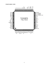
TAS5508
8-Channel
Digital Audio PWM Processor
SLES091C
–
FEBRUARY
2004–
REVISED AUGUST
2005
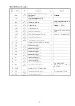
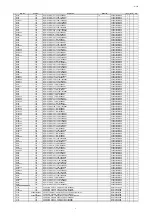
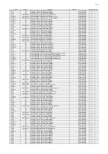
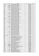
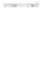
TERMINAL
5-V
TYPE
(1)
TERMINATION
(2)
DESCRIPTION
TOLERANT
NAME
NO.
PWM_P_3
45
DO
PWM 3 output
(differ)
PWM_P_4
47
DO
PWM 4 output
(differ)
PWM_P_5
56
DO
PWM 5 output
(differ)
PWM_P_6
58
DO
PWM 6 output
(differ)
PWM_P_7
50
DO
PWM 7
(lineout L)
output
(differ)
PWM_P_8
52
DO
PWM 8
(lineout R)
output
(differ)
RESERVED
21, 22,
Connect
to digital ground
23, 64
RESET
11
DI
5 V
Pullup
System reset input, active-low. A system reset is generated
by
applying a logic
low to this terminal.
RESET
is an asynchronous control signal that restores the
TAS5508
to its default conditions, sets the valid output low, and places the
PWM in the hard mute
(M)
state. Master volume is immediately set to full
attenuation. On the release of
RESET
, if
PDN
is high, the system performs a 4-
to 5-ms device initialization and sets the volume at mute.
SCL
25
DI
5 V
I
2
C
serial-control clock input/output
SCLK
27
DI
5 V
Serial-audio data clock
(shift clock)
input
SDA
24
DIO
5 V
I
2
C
serial-control data-interface input/output
SDIN1
31
DI
5 V
Pulldown
Serial-audio data input 1 is one of the serial-data input ports.
SDIN1
supports
four discrete
(stereo)
data formats and is
capable
of inputting data at 64 Fs.
SDIN2
30
DI
5 V
Pulldown
Serial-audio data input 2 is one of the serial-data input ports.
SDIN2
supports
four discrete
(stereo)
data formats and is
capable
of inputting data at 64 Fs.
SDIN3
29
DI
5 V
Pulldown
Serial-audio data input 3 is one of the serial-data input ports.
SDIN3
supports
four discrete
(stereo)
data formats and is
capable
of inputting data at 64 Fs.
SDIN4
28
DI
5 V
Pulldown
Serial-audio data input 4 is one of the serial-data input ports.
SDIN4
supports
four discrete
(stereo)
data formats and is
capable
of inputting data at 64 Fs.
VALID
39
DO
Output indicating validity of PWM outputs, active-high
VBGAP
10
P
Band-gap voltage reference. A pinout of the internally regulated 1.2-V reference.
Typically
has a 1-nF
low-ESR
capacitor
between
VBGAP and
AVSS_PLL. This
terminal must not
be
used to power
external
devices.
VR_DIG
33
P
Voltage reference for 1.8-V digital core supply. A pinout of the internally
regulated 1.8-V power used
by
digital core logic. A 4.7-
µ
F
low-ESR
capacitor
(3)
should
be
connected
between
this terminal and DVSS.
This
terminal must not
be
used to power
external
devices.
VR_DPLL
17
P
Voltage reference for 1.8-V digital
PLL
supply. A pinout of the internally
regulated 1.8-V power used
by
digital
PLL
logic. A 0.1-
µ
F
low-ESR
capacitor
(3)
should
be
connected
between
this terminal and
DVSS_CORE. This
terminal
must not
be
used to power
external
devices.
VR_PWM
48
P
Voltage reference for 1.8-V digital PWM core supply. A pinout of the internally
regulated 1.8-V power used
by
digital PWM core logic. A 0.1-
µ
F
low-ESR
capacitor
(3)
should
be
connected
between
this terminal and
DVSS_PWM. This
terminal must not
be
used to power
external
devices.
VRA_PLL
1
P
Voltage reference for 1.8-V
PLL
analog supply. A pinout of the internally
regulated 1.8-V power used
by PLL
logic. A 0.1-
µ
F
low-ESR
capacitor
(3)
should
be
connected
between
this terminal and
AVSS_PLL. This
terminal must not
be
used to power
external
devices.
VRD_PLL
7
P
Voltage reference for 1.8-V
PLL
digital supply. A pinout of the internally
regulated 1.8-V power used
by PLL
logic. A 0.1-
µ
F
low-ESR
capacitor
(3)
should
be
connected
between
this terminal and
AVSS_PLL. This
terminal must not
be
used to power
external
devices.
XTL_IN
20
AI
XTL_OUT
and
XTL_IN
are the only
LVCMOS
terminals on the device.
They
provide a reference clock for the
TAS5508
via use of an
external
fundamen-
tal-mode crystal.
XTL_IN
is the 1.8-V input port for the oscillator circuit. A
13.5-MHz crystal
(HCM49)
is recommended.
XTL_OUT
19
AO
XTL_OUT
and
XTL_IN
are the only
LVCMOS
terminals on the device.
They
provide a reference clock for the
TAS5508
via use of an
external
fundamen-
tal-mode crystal.
XTL_OUT
is the 1.8-V output drive to the crystal. A 13.5-MHz
crystal
(HCM49)
is recommended.
(3)
If desired,
low-ESR
capacitance values can
be
implemented
by
paralleling two or more ceramic capacitors of equal value. Paralleling
capacitors of equal value provides an
extended
high-frequency supply decoupling.
This
approach avoids the potential of producing
parallel resonance circuits that have
been observed
when paralleling capacitors of different values.
Description
19
Summary of Contents for CEOL RCD-N8
Page 10: ...10 DIMENSION 299 0 112 0 108 0 35 0 35 0 210 0 280 0 2 0 301 0 218 0 45 0 36 0 30 0 4 0 ...
Page 22: ...22 3 Remove the screws 4 Remove the screws Shooting direction C Shooting direction A ...
Page 24: ...24 4 Remove the screws remove the connector wires CN221 CN222 Shooting direction C ...
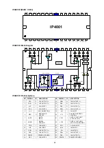
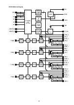
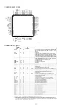
Page 84: ...84 PCM9211 MAIN IC103 ...
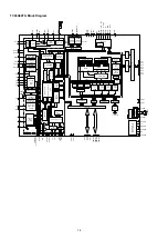
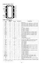
Page 85: ...85 PCM9211 Block Diagram ...
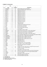
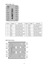
Page 86: ...86 PCM9211 Pin Discriptions ...
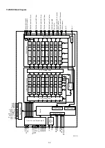
Page 87: ...87 NJM2755 MAIN IC701 NJM2755 Block Diagram ...
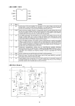
Page 93: ...93 L6565 SMPS IC821 L6565 Block Diagram ...
Page 94: ...94 ICE3BR1765J SMPS IC871 ICE3BR1765J Block Diagram ...


