


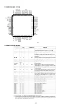


82
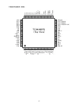
TC94A92FG
2009-05-27
8
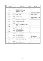
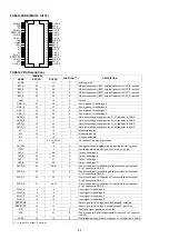
Pin
No.
Symbol I/O
Description
Default
Remarks
61
VDD3
-
Power Supply pin for 3.3V Digital circuit
-
62
BUS0
I/O
3I/F
Microprocessor I/F data input/output pin 0
I
CMOS Port
Schmitt input
Refer to [1.2 Pin Assinment Table]
63
BUS1
I/O
3I/F
Microprocessor I/F data input/output pin 1
I
CMOS Port
Schmitt input
Refer to [1.2 Pin Assinment Table]
64
BUS2
I/O
3I/F
Microprocessor I/F data input/output pin 2
I
CMOS Port
Schmitt input
Refer to [1.2 Pin Assinment Table]
65
BUS3
I/O
3I/F
Microprocessor I/F data input/output pin 3
I
CMOS Port
Schmitt input
Refer to [1.2 Pin Assinment Table]
66
BUCK
I
3I/F
Microprocessor I/F BUS clock Input pin
I
Schmitt input
Refer to [1.2 Pin Assinment Table]
67
/CCE
I
3I/F
Microprocessor I/F chip enable input pin
I
Schmitt input
Refer to [1.2 Pin Assinment Table]
68
MS
I
3I/F
Microprocessor I/F mode selection pin.
“H”: Parallel I/F, “L”: Serial I/F
I
Refer to [1.2 Pin Assinment Table]
69
/RST
I
3I/F
Reset Input pin
I
Schmitt input
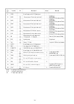
70
Test
I
3I/F
Test pin
(
”L” fixed
)
I
Connect to GND for normal operation
71
VDD1-1
-
Power Supply pin for 1.5V Digital circuit
-
72
VSS-1
-
Grounding pin for 1.5V Digital circuit
-
73
/SRAMSTB
I
3I/F
1Mbit SRAM stand by pin
(
/SRAMSTB="L"
)
I
74
VDDM1
-
Power Supply for 1.5V 1Mbit SRAM circuit
-
75
PDo
O
3AI/F
EFM and PLCK Phase difference signal output pin.
O
4-state output ( RVDD3,
RVSS3,PVREF, Hiz)
76
TMAX
O
3AI/F
TMAX detection result output pin
O
3-state output ( RVDD3, RVSS3, Hiz)
77
LPFN
I
3AI/F
PLL circuit LPF amplifier inversion input pin
I
78
LPFo
O
3AI/F
PLL circuit LPF amplifier Output pin
O
79
PVREF -
PLL circuit 1.65 V reference voltage pin.
-
Connected to VRO. Connect to
GND by 0.1uF and 100uF.
80
VCoF
O
3AI/F
VCO filter pin
O
Connect to GND by 0.01uF
3A I/F
: 3 V analog circuit input/output pin.
1.5 I/F
: 1.5Vdigital input/output pin.
3 I/F
: 3 V digital input/output pin
.
Summary of Contents for CEOL RCD-N8
Page 10: ...10 DIMENSION 299 0 112 0 108 0 35 0 35 0 210 0 280 0 2 0 301 0 218 0 45 0 36 0 30 0 4 0 ...
Page 22: ...22 3 Remove the screws 4 Remove the screws Shooting direction C Shooting direction A ...
Page 24: ...24 4 Remove the screws remove the connector wires CN221 CN222 Shooting direction C ...
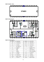
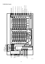
Page 84: ...84 PCM9211 MAIN IC103 ...
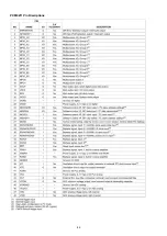
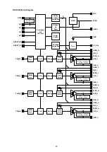
Page 85: ...85 PCM9211 Block Diagram ...
Page 86: ...86 PCM9211 Pin Discriptions ...
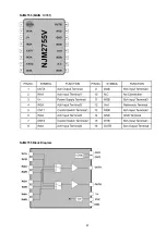
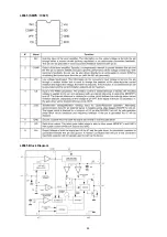
Page 87: ...87 NJM2755 MAIN IC701 NJM2755 Block Diagram ...
Page 93: ...93 L6565 SMPS IC821 L6565 Block Diagram ...
Page 94: ...94 ICE3BR1765J SMPS IC871 ICE3BR1765J Block Diagram ...


