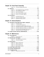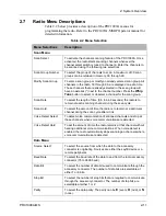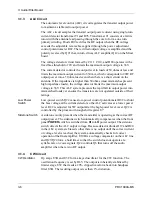
2: System Overview
PRC1099A-MS
2-9
Driver amplifier
bias voltage
circuit - U3, Q6
Transmit
Provide temperature adjusted
bias voltage to driver amplifiers
Q2 and Q3.
Inputs thermally-compensated
voltage from D1.
Outputs bias voltage to driver
amplifiers Q2 and Q3.
Power amplifier
bias voltage
circuit - U4, Q7
Transmit
Provide temperature adjusted
bias voltage to driver amplifiers
Q4 and Q5.
Inputs thermally-compensated
voltage from D2.
Outputs bias voltage to driver
amplifiers Q4 and Q5.
Antenna Tuner Board
Antenna Tuner -
matching network
(C1, C2, C5, and
L1–L10)
Relays K1–K10,
K13, K15 and K17
Transmit
Translates 20W RF output signal
at selected channel frequency
through matching network for
maximum power transfer.
Inputs transmit signal at the
selected channel frequency from
low-pass filters on the Audio/Filter
board.
Outputs to either whip antenna or
50 Ohm front panel antenna
connector.
Receive
Translates 20W RF input signal at
selected channel frequency
through matching network for
maximum power transfer.
Input receive signal at the select
channel frequency from either
whip antenna or 50 Ohm front
panel antenna connector.
Outputs receive signal at selected
channel frequency to low-pass
filters on the Audio/Filter board.
Serial Decoders
and Relay Drivers
- U2, U3, U4
N/A
Selects inductors or capacitors to
insert into either transmit or
receive signal paths for maximum
power transfer.
Inputs serial data from the
Processor board.
Outputs control signal to latching
relays.
Synthesizer Board
First LO - DDS U9 N/A
76.50 to 105.00 MHz
Outputs LO1 frequency to 1st LO
buffer Q1 on Mixer board.
Second LO - DDS
U9
N/A
73.35 MHz
Outputs LO2 frequency to 2nd LO
buffer Q10 on Mixer board.
BFO - DDS U9
N/A
1650 kHz or 1647 kHz
Outputs BFO frequency to
balanced modulator U6 and
product detector U4 on
Audio/Filter board.
Serial Decoders
N/A
Input from Processor board.
Processor Board
Serial bus
N/A
Transports data to various control
and processing devices on
different boards.
Input from processor.
Output to all serial ports.
Control Switches
N/A
Read by processor.
Table 2-1 Board Functionality (continued)
Function
Path
Description
I/O


