background image

CNT24-4(PCI)

Setup

17

For installing the third board and later, follow the same steps as
those for installing the second one.  Before you can install the
third board or later, all of the already installed CNT24-4(PCI)
boards must be in the PCI bus slots.

Notes!

- The second CNT24-4(PCI) board cannot be installed normally

unless the resources (I/O addresses and interrupt level) to be
used for the board cannot be allocated.  Before trying to install
the second board, check free resources on the personal computer.

- The resources used for each CNT24-4(PCI) board do not depend

on the location of the PCI bus slot or the board itself.  If you
remove two or more CNT24-4(PCI) boards which have already
been installed and then re-mount one of them on the computer,
therefore, it is unknown which one of the sets of resources
previously assigned to the two boards is assigned to the re-
mounted board.  In this case, check the resource settings again.

Summary of Contents for CNT24-4

Page 1: ...CNT24 4 PCI 24Bit Up Down Counter Board for PCI User s Guide ...

Page 2: ...nge without notice All relevant issues have been considered in the preparation of this document Should you notice an omission or any questionable item in this document please feel free to notify CONTEC Co LTD Regardless of the foregoing statement CONTEC assumes no responsibility for any errors that may appear in this document nor for results obtained by the user as a result of using this product T...

Page 3: ... bag to prevent damage in shipping Check the contents to make sure that you have everything listed above If you do not have all the items contact your distributor or CONTEC group office where you purchased Note Do not remove the board from its protective packaging until the computer case is open and ready for installation Electrical static can cause damage to electrical components ...

Page 4: ... 1 8 Procedure 8 Checking resources 8 Obtaining resource information 9 Sample programs for MS DOS 9 Sample s Specification 10 Setting up the Board for Use under Windows 95 14 Checking the OS version 14 Procedure for use under Windows 95 version 4 00 950 or 4 00 950a 15 Procedure for use under Windows 95 version 4 00 950B 15 Method of installing two or more CNT24 4 PCI boards for use under Windows ...

Page 5: ...30 Measures Against Voltages 31 4 I O Ports and Registers 33 I O Port Bit Assignment 33 Data Setting 33 Count Value Flow 34 Operation Command 35 Output Command 37 Count initial value Commands CH0 00h CH1 05h CH2 0Ah CH3 0Fh 37 Operation Mode Command CH0 01h CH1 06h CH2 0Bh CH3 10h 37 Counter Operation Mode 40 2 phase input 40 Single phase input 40 Single phase input with gate control 41 Synchroniz...

Page 6: ...ncy 51 One shot pulse Command 19h 52 Input Command 53 Read count value Command CH0 00h CH1 05h CH2 0Ah CH3 0Fh 53 Status data Command CH0 01h CH1 06h CH2 0Bh CH3 10h 54 Interrupt mask Command 15h 56 Sense port Command 16h 56 Default Setting 57 5 System Reference 59 Specifications 59 Block Diagram 60 6 Troubleshooting 61 QUESTIONS 61 Is the pilot light on 61 Did the system boot up 61 Does your prog...

Page 7: ...nterface Connector 23 Figure 3 2 CN1 Connector as Viewed from Back of Computer 24 Figure 3 3 CN1 Pin Assignments 24 Figure 3 4 CN2 Frontal View 25 Figure 3 5 CN2 Pin Assignments 25 Figure 3 6 Optional Cable DT B2 26 Figure 3 7 37 Pin D Type Connector Pin Assignments 26 Figure 3 8 Digital Input 27 Figure 3 9 Connecting to Open collector Output Device 27 Figure 3 10 TTL Level Input Circuitry 28 Figu...

Page 8: ... Example 40 Figure 4 6 Example of Single phase Input with Gate Control 41 Figure 4 7 Example of Synchronization Clear 42 Figure 4 8 Example of Asynchronization Clear 42 Figure 4 9 Counting Example for Multiplied Count Inputs 43 Figure 4 10 Number of Z phase Inputs Available ZSE 0 Positive Logic 44 Figure 4 11 Digital Filter 47 Figure 5 1 Block Diagram 60 ...

Page 9: ...Counter Operation Mode 38 Table 4 4 Switching Counting Direction 39 Table 4 5 Z phase Input Mode 44 Table 4 6 Digital Filter Clock Data 47 Table 4 7 Relationship between programmable timer interrupt 51 Table 4 8 Relationship Between One shot Pulse Width Data and Pulse Width 52 Table 4 9 Default Setting 57 Table 5 1 Specifications 59 ...

Page 10: ...tion programs and connecting the required external devices to the board Features One board enables 24 bit up down counts for four channels Counts two phase signals from devices like a rotary encoder or a linear gauge Photocoupler insulated input or TTL level input for each channel Generates interrupts or outputs signals by matching the count value of each channel with the value set by the user Per...

Page 11: ... if the device has been tampered with or damaged through abuse mistreatment neglect or unreasonable use or if the original invoice is not included in which case repairs will be considered beyond the warranty policy How to Obtain Service For replacement or repair return the device freight prepaid with a copy of the original invoice Please obtain a Return Merchandise Authorization Number RMA from th...

Page 12: ...ts switches Chapter 3 Connecting the External Devices This chapter explains how to connect external devices to the board and gives notes on connecting them Chapter 4 I O Ports and Registers This chapter provides the assignment and definitions of each I O port bit used the board Chapter 5 Specifications This chapter summarizes the hardware specifications of the board and provides circuit block diag...

Page 13: ...Introduction CNT24 4 PCI 4 ...

Page 14: ...ing shown below is the factory default Interface connector for photocoupler resistance input CN1 CNT24 4 PCI SW1 BOARD ID SW1 BOARD ID Setting Switch BOARD ID 0 1 2 3 4 5 6 7 9 A B C D E F 8 Jumper for interrupt signal resource settings Interface connector for TTL level input CN2 JP1 1 2 3 INT USE NOT USE JP1 Figure 2 1 Component Locations ...

Page 15: ... the boards The board IDs from 0 to F can be set to identify up to sixteen boards If only one board is used the original factory setting Board ID 0 should be used Setting procedure To set the board ID use the rotary switch on the board Turn the SW1 knob to set the board ID as shown below SW1 BOARD ID 0 1 2 3 4 5 6 7 9 A B C D E F 8 Same for match output BOARD ID 0 Figure 2 2 Board ID Settings SW1 ...

Page 16: ...C you can let recognize to the PC the CNT24 4 PCI as no Interrupt function boards In case of interrupt use this board is assigned the interrupt level from PC Setup when interrupt is used JP1 INT USE NOT USE Factory setting Setup when interrupt is not used JP1 INT USE NOT USE 1 2 3 1 2 3 Figure 2 3 Setting the Interrupt Use ...

Page 17: ... DOS gets and running When setting up the board has been completed be sure to check the assigned resources Checking resources Before operating the CNT24 4 PCI board be sure to check the personal computer resources I O addresses and interrupt level assigned to the board For PCI compatible Plug and Play compliant boards free resources among the personal computer resources are assigned automatically ...

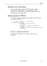
Page 18: ...ams for MS DOS The sample programs for using the CNT24 4 PCI under MS DOS are written in Microsoft C 1 CNTPCI C Resource check program CNTPCI EXE 2 CNTPCI01 C Count value of any Channel CNTPCI01 EXE 3 CNTPCI02 C 4 channel count value at the same time CNTPCI02 EXE 4 CNTPCI03 C Count value for every time period by timer interrupt CNTPCI03 EXE DOS Samples DOS Samples 98 or PC Figure 2 4 Sample Progra...

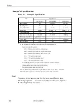
Page 19: ...data example 8Ch Photocoupler insulation 2 phase input 9Bh Photocoupler insulation Single phase input 8Bh Photocoupler insulation Gate control input CCh TTL level 2 phase input DBh TTL level Single phase input CBh TTL level Gate Control input Other settings Common Asynchronization clear UP counting direction Z phase positive logic Single input multiplication The Sample program uses the 8C setting ...

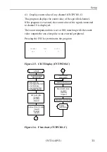
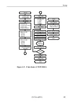
Page 20: ...ts the one shot pulse to an external peripheral Pressing the ESC key terminates the program CHANNEL DATA STATUS CH0 0 7F Figure 2 5 CRT Display CNTPCI01 C START 1 Initial setting Set operation mode Set Z phase Set digital filter Reset sense bit Set count data Lower Middle Upper 1 Set I O address Set channel Latch count value Calculate count value Set count match data Lower Middle Upper Set one sho...

Page 21: ...02 C 3 Display count value for every time period by timer interrupt CNTPCI03 C This program generates an interrupt every second using the timer and displays the count value If this program is executed the count values HEX and decimal of the signal that is connected to channels 0 3 are displayed The interrupt level is IRQ5 Pressing the ESC key terminates the program CHANNEL DATA CH0 0 DATA HEX 0000...

Page 22: ...r Reset sense bit END Save registar Input number of timer count ups Interrupt EQI process Restore register IRET END Set IMR N Y Set address Set count data Lower Middle Upper Set count data Lower Middle Upper Clear mask Set timer data Lowest Lower Upper Highest Check sense port Read count value Calculate count value Display count value Stop timer Figure 2 9 Flowcharts CNTPCI03 C ...

Page 23: ...f hardware in Windows 95 is called installing the hardware Use the appropriate procedure to install the CNT24 4 PCI Checking the OS version Note that the procedure for installing the CNT24 4 PCI is different depending on each version of Windows 95 Check the version of Windows 95 on your system as follows before installing the CNT24 4 PCI 1 Open Control Panel from My Computer 2 Double click on the ...

Page 24: ...tion of the CNT24 4 PCI After finishing installing the board be sure to check the assigned resources Procedure for use under Windows 95 version 4 00 950B 1 Set the board ID 2 Be sure to check that the personal computer is off then plug the board into a PCI bus slot in the personal computer 3 Turn the personal computer on to start up Windows 95 4 Windows 95 will come up with the New Hardware detect...

Page 25: ...rd ID of the second CNT24 4 PCI board then plug it into a PCI bus slot To the second board assign a board ID different from that assigned to the first board 5 Turn the personal computer on again to start up Windows 95 6 Windows 95 will come up with the New Hardware detection dialog box In Multimedia Device Select which driver you want to install for your new hardware select Select from List 7 The ...

Page 26: ...t level to be used for the board cannot be allocated Before trying to install the second board check free resources on the personal computer The resources used for each CNT24 4 PCI board do not depend on the location of the PCI bus slot or the board itself If you remove two or more CNT24 4 PCI boards which have already been installed and then re mount one of them on the computer therefore it is un...

Page 27: ...the first board before trying to install the second one 3 Exit Windows 95 and turn the personal computer off 4 Check the board ID of the second CNT24 4 PCI board then plug it into a PCI bus slot To the second board assign a board ID different from that assigned to the first board 5 Turn the personal computer on again to start up Windows 95 6 The OS will then automatically install the second board ...

Page 28: ...sses and interrupt level assigned to the board For PCI compatible Plug and Play compliant boards free resources among the PC resources are assigned automatically upon activation of the personal computer Follow the steps below to check the assigned resources managed by the OS 1 Double click on the System option in Control Panel to open the System Properties property sheet Select the Device Manager ...

Page 29: ...s 95 API CNT 98 PC W95 Ver 2 3 or later These pieces of driver software support up to four CNT24 4 PCI boards Note that when API CNT 98 PC W95 is used development languages that can be used are only 32 bit versions Neither driver can be supported by any language dedicated to 16 bit applications ...

Page 30: ...ardware Installing the CNT24 4 PCI board requires separately priced CONTEC driver software API CNT 98 PC NT Follow the procedure below to install the board Procedure 1 Set the board ID 2 Be sure to check that the personal computer is off then plug the board into a PCI bus slot in the personal computer 3 Turn the personal computer on to start up Windows NT 4 When Windows NT has been started run SET...

Page 31: ...onal computer Follow the steps below to check the assigned resources managed by the OS 1 Open Windows NT Diagnostic Program from Management Tools 2 Select Resources IRQ port settings Check the type and settings of resources assigned to the API CNT 98 PC NT and the conflicting device list Once the CNT24 4 PCI has been installed correctly it can be used under Windows NT Support software CONTEC provi...

Page 32: ...ctor on the board Use CN1 for the photocoupler insulated input For TTL level input connect CN2 to an external device by connecting the optional cable to CN2 Matched pulse output is output from CN1 Photocoupler insulated open collector output Figure 3 1 Connecting the Interface Connector Note See Chapter 3 Option cable DT B2 for further information ...

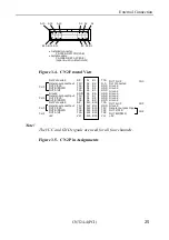
Page 33: ...eneral purpose Input OUT Z CLR OUT B DOWN OUT A UP Plus Common 2 Not Connected Minus Common CH3 Output CH2 Output CH1 Output CH0 Output Plus Common 19 18 17 16 15 14 13 12 11 10 9 8 7 6 5 4 3 2 1 37 36 35 34 33 32 31 30 29 28 27 26 25 24 23 22 21 20 P3P P3U P3Z P3B P3A N C P2U P2Z P2B P2A P2P N C OUTN OUT3 OUT2 OUT1 OUT0 OUTP N C P1P P1U P1Z P1B P1A N C P0U P0Z P0B P0A P0P N C N C N C N C N C N C ...

Page 34: ...eneral purpose Input OUT Z CLR OUT B DOWN Not Connected General purpose Input OUT Z CLR OUT B DOWN OUT A UP 5V CH0 N C T1U T1Z T1B T1A GND T0U T0Z T0B N C T3U T3Z T3B T2A Vcc CH0 CH2 A1 A2 A3 A4 A5 A6 A7 A8 A9 A10 A11 A12 A13 A14 A15 T0A N C GND GND GND GND GND GND GND T3A GND T2U T2Z T2B Vcc OUT A UP Not Connected Ground Ground Ground Ground Ground Ground Ground OUT A UP Ground General purpose In...

Page 35: ...1 22 23 24 25 26 27 28 29 30 31 32 33 34 35 36 37 Vcc Vcc N C N C N C N C N C N C T2A T2B T2Z T2U GND T3A T3B T3Z T3U N C CH0 Ground Not connected OUT A UP OUT B DOWN OUT Z CLR General purpose Input Ground OUT A UP OUT B DOWN OUT Z CLR General purpose Input Not connected Not connected CH1 5V 5V Not connected OUT A UP OUT B DOWN OUT Z CLR General purpose Input Ground OUT A UP OUT B DOWN OUT Z CLR G...

Page 36: ...B I O connector on the board Figure 3 8 shows Digital input circuits Figure 3 9 shows an example of connecting this board to open collector output device 220Ω Photocoupler 2 2kΩ BOARD Digital output Input Terminal 5V Plus common External Signal Output Figure 3 8 Digital Input 220Ω 2 2kΩ 12V 400Ω Photocoupler Input Terminal R Plus common External Signal Output Figure 3 9 Connecting to Open collecto...

Page 37: ...ing resistor Assume external power is PV then 20 Rk Ω 15 P 5 P 5 If P 12 use a 350 R 470 ohm resistor Diode Vcc 5V GND LS244 BOARD Digital output Input Terminal External Signal Output Diode Figure 3 10 TTL Level Input Circuitry Notes The general input signal uses the same circuit structure The cable should be 1 5m or less To prevent malfunction caused by noise separate the circuit as much as possi...

Page 38: ...sult an external power source is needed to run the board output Photocoupler 1kΩ Plus common 1kΩ External Power Supply DC5V 12V Vcc 18kΩ Photocoupler Load Load Output pin Minus common Figure 3 11 Output Circuit and Connecting Example Note The board s output transistor does not have a surge voltage protection circuit As a result to run inductive loads for example relays and lamps install surge volt...

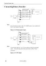
Page 39: ... To use the photocoupler with 12V 400Ω resistors are needed at R For 5V no resistor is needed Figure 3 12 Photocoupler Input Connector pin number CH0 9 CH2 28 CH1 14 CH3 33 CNT24 4 PCI CN2 0V CH0 10 CH2 29 CH1 15 CH3 34 CH0 11 CH2 30 CH1 16 CH3 35 Option Cable GND 1 7 13 32 CN2 A phase B phase Z phase A phase B phase Z phase Power source Shield Encoder Note Convert the connector to a 37 pin connec...

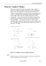
Page 40: ...ough a coil including a relay causes the sudden generation of a high voltage pulse If its voltage exceeds the withstand voltage of the transistor the performance of the transistor may be degraded or it may be damaged To prevent this be sure to connect a surge absorption element when driving an inductive load including a relay coil Examples of measures against surge voltages are as shown in the Fig...

Page 41: ...External Connection CNT24 4 PCI 32 ...

Page 42: ... an OUT command every time for the output port 0 The following Figure 4 1 and Figure 4 2 show the I O port bit allocation Base Address Command output select register Setting data output D7 D6 D5 D4 D3 D2 D1 D0 0 1 2 3 Not use Not use Figure 4 1 Output port Base Address Impossible Data status read D7 D6 D5 D4 D3 D2 D1 D0 0 1 2 3 Not use Not use Figure 4 2 Input port Data Setting To set 8 bit data e...

Page 43: ...er Latch count value Command 14h Command CH0 00h CH1 05h CH2 0Ah CH3 0Fh Coincidence signal Sense port Command 16h Interrupt mask Command 15h Command CH0 01h CH1 06h CH2 0Bh CH3 10h Status data Output one shot pulse Command 19h Command CH0 03h CH1 08h CH2 0Dh CH3 12h Read Regisster Read Counter value Count value coincidence Set comparison register Figure 4 3 Count Value Flow ...

Page 44: ...igital filter CH1 Digital filter 0A CH2 Count initial value CH2 Count initial value 0B RESET SEL ZSEL UD AB DIR SEL2 SEL1 SEL0 CH2 Operation mode 0C No used ZE1 ZE0 0 CH2 Z phase CLR input 0D CH2 count compare value CH2 Comparison register 0E No used Clock data for digital filter CH2 Digital filter 0F CH3 Count initial value CH3 Count initial value 10 RESET SEL ZSEL UD AB DIR SEL2 SEL1 SEL0 CH3 Op...

Page 45: ...Q U CH0 Status data 8 05 CH1 read count value CH1 Read count value 24 06 AI Z A B 1 U D EQ U CH1 Status data 8 0A CH2 read count value CH2 Read count value 24 0B AI Z A B 1 U D EQ U CH2 Status data 8 0F CH3 read count value CH2 Read count value 24 10 AI Z A B 1 U D EQ U CH2 Status data 8 15 0 0 0 TIME CH3 CH2 CH1 CH0 Interrupt mask 5 16 0 0 0 TIME CH3 CH2 CH1 CH0 Sense port 5 ...

Page 46: ...count initial value The following sample program shows how to set the count initial value 100 64h in CH0 OUT Address 0h 00h CH0 Select count data OUT Address 1h 64h Lower bits OUT Address 1h 00h Middle bits OUT Address 1h 00h Upper bits Operation Mode Command CH0 01h CH1 06h CH2 0Bh CH3 10h D7 D6 D5 D4 D3 D2 D1 D0 01h 06h 0Bh 10h UD AB SEL SEL2 SEL1 SEL0 DIR RESET ZSEL Execute an OUT command for o...

Page 47: ...chronization clear Single multiplication mode 2 phase input Synchronization clear Double multiplication mode 2 phase input Synchronization clear Quadruple multiplication mode 2 phase input Asynchronization clear Single multiplication mode See 2 phase input Asynchronization clear Table4 4 Double multiplication mode 2 phase input Asynchronization clear Single multiplication mode Single phase input A...

Page 48: ...isters 39 DIR Switches The rotary encoder counting direction Table 4 4 Switching Counting Direction Rotary encoder rotation Clockwise Counterclockwise 0 DOWN UP 1 UP DOWN DIR Note In the default setting all of channels are set 00h ...

Page 49: ... phase CLR Counting 0 1 2 Figure 4 4 Counting Example with 2 phase Input Single phase input For a single phase input the counter counts up with an UP pulse and counts down with a DOWN pulse If UP and DOWN pulses occur at the same time or both pulses are LOW the counter will not count properly UP pulse A phase UP DOWN pulse B phase DOWN Counting 6 7 8 5 6 7 Figure 4 5 Single phase Counting Example ...

Page 50: ...to zero Single pulse A phase UP Gate control signal B phase DOWN no count Couting 7 8 6 9 Figure 4 6 Example of Single phase Input with Gate Control Note This is a counting operation when DIR 1 If DIR 0 and the gate control signal B phase DOWN is HIGH the counter counts down with the rising edge of a single phase pulse A phase UP If DIR 0 and the gate control signal is LOW the counter stops ...

Page 51: ...g down with a rising edge of an A phase input If ZSEL 0 the Z phase input is available only when it is LOW Asynchronization clear If DIR 1 ZSEL 1 regardless of the input state of the A phase and B phase inputs the counter is zero cleared when a Z phase input changes to HIGH and regardless of the Z phase input state the counter starts counting with the next rising edge of the A phase input A phase ...

Page 52: ...s double or quadruple more precise counting is available Double phase input Single phase input For single phase input only the single multiplication mode is available There is no double or quadruple multiplication Single phase input with gate control Figure 4 9 Counting Example for Multiplied Count Inputs ...

Page 53: ...puts on output port 1 ZE1 ZE0 Select Z phase input mode Table 4 5 Z phase Input Mode ZE1 ZE0 State 0 1 Disable Z phase input if there is no Z phase input 1 0 Only the next Z phase input is available 1 1 Every Z phase input is available mark is the default setting Disabled Z phase input Only next Z phase input is available Every Z phase input is available Figure 4 10 Number of Z phase Inputs Availa...

Page 54: ...channel and the data in the comparison register are compared If they match the status bit EQ is set to 0 As long as they match the bit remains 0 This register is cleared when the bus is reset Output the command on the output port 0 and set the comparison data on the output port 1 The comparison data is 24 bit data Output the data three times eight bits at a time from the lower bits the middle bits...

Page 55: ...with the sampling clock if it detects HIGH or LOW signals for four consecutive clocks it outputs a HIGH or LOW signal and sends the signal to the counter circuit Output a command to output port 0 and set the sampling frequency on the output port 1 The range is 100nsec 1056 1 usec Note Since external input signals except the general input signal are read into the internal counter through the digita...

Page 56: ... 1 32 1µsec 3 0 1 0 0 204 9µsec 480Hz 0 1 0 1 211 3µsec 470Hz 0 1 1 0 230 5µsec 430 0 1 1 1 236 9µsec 420 1 0 0 0 819 3µsec 122 1 0 0 1 825 7µsec 121 1 0 1 0 844 9µsec 118 1 0 1 1 851 3µsec 117 1 1 0 0 1024 1µsec 97 1 1 0 1 1030 5µsec 96 1 1 1 0 1049 7µsec 95 1 1 1 1 1056 1µsec 94 The accuracy is 0 01 of the setting frequency Notes The default is 100nsec setting Some noise causes more than a four ...

Page 57: ...D0 15h TIME Not used CH2 CH1 CH0 CH3 Output 15h to output port 0 and set the mask on output port 1 By setting an appropriate bit to 1 the interrupt is disabled TIME Setting this bit to 1 disables the interrupt that signals that the programmable timer has elapsed for the predetermined time Setting this bit to 0 enables the interrupt CH3 CH0 These bits correspond to the channels Setting these bit to...

Page 58: ...nding bit changes 1 If this bit is 1 the interrupt does not occur with the next count match or the timer count is up Outputting 16h to output port 0 and outputting 1 to the corresponding bit of output port 1 clear the sense bit The next interrupt signal can be generated TIME Resets the sense bit when the programmable timer count is up CH3 CH0 Resets the sense bit for count match of the channels ...

Page 59: ...t the data four times eight bits at a time from the lower bits to the upper bits The range is 1msec 200sec To start the timer output the timer start command 18h and set the corresponding bit on output port 1 Setting the bit to 0 stops the timer Table 4 8 shows the relationship between the programmable timer data and the timer interrupt frequency Example The following program sample show how to set...

Page 60: ...byte Low byte frequency 0 0 0 0 4 E 1 F 1msec 0 0 0 3 0 D 3 F 10msec 0 0 1 E 8 4 7 F 100msec 0 1 3 1 2 C F F 1sec 0 2 6 2 5 9 F F 2sec 0 3 9 3 8 6 F F 3sec 0 4 C 4 B 3 F F 4sec 0 5 F 5 E 0 F F 5sec 0 7 2 7 0 D F F 6sec 0 8 5 8 3 A F F 7sec 0 9 8 9 6 7 F F 8sec 0 A B A 9 4 F F 9sec 0 B E B C 1 F F 10sec 1 1 E 1 A 2 F F 15sec 1 7 D 7 8 3 F F 20sec 2 3 C 3 4 5 F F 30sec 2 F A F 0 7 F F 40sec 3 B 9 A ...

Page 61: ... 4 8 Relationship Between One shot Pulse Width Data and Pulse Width One shot pulse width data D7 D0 h Pulse width 0 0 0 0 0 0 0 0 00h 0 0 0 0 0 0 0 0 1 01h About 409 6µsec 0 0 0 0 0 0 1 0 02h About 819 2µsec 0 0 0 0 0 0 1 1 03h About 1 23msec 0 0 0 0 1 1 0 0 0Ch About 4 92msec 0 0 0 1 1 0 0 1 19h About 10 24msec 0 0 1 1 0 0 0 1 31h About 20 07msec 0 1 0 0 1 0 0 1 49h About 29 9msec 0 1 1 0 0 0 1 0...

Page 62: ...d To read the count output the command to output port 0 and read input port 1 three times lower middle and upper bits The default of the read out register is not determined The following sample program shows how to read the CH2 counter value OUT Address 0 0Ah Select CH2 count data IN Address 1 Lower bits IN Address 1 Middle bits IN Address 1 Upper bits Note First set the CH2 data latch to 1 ...

Page 63: ... the same time 1 Invalid input 0 No invalid input Z This bit shows the Z phase input status Positive logic 1 Z phase input status 1 0 Z phase input status 0 Negative logic 1 Z phase input status 0 0 Z phase input status 1 A This bit shows the A phase input status 1 A phase input status 1 0 A phase input status 0 B This bit shows the B phase input status 1 B phase input status 1 0 B phase input sta...

Page 64: ...eral input status 0 Notes The default changes depending on the external connection status Since the status data of A phase B phase and Z phase is the data after the filtering process it has a 4 clock delay in the frequency that has been set Z phase logic is set by the ZSEL of the operation mode setting ...

Page 65: ...H2 CH1 CH0 CH3 This shows the channel count match and count up To monitor the sense port output 16h to output port 0 and read input port 1 TIME This bit is set to 1 when the time set in the program mable timer has elapsed CH3 CH0 For any channel between CH3 CH0 when a value in the up down counter and the comparison register matches the bit for the channel is set to 1 The interrupt channel is deter...

Page 66: ...ing Item Default setting Operation mode 00h Z phase CLR input 04h Comparison register 0 Read register unfixed 24 bit up down counter 000000h Digital filter 00h 0 1µsec Status data 7Bh not connected for external Latch count value 00h Interrupt mask 1Fh all disable Sense port 00h Timer data 00000000h Timer start 00h stop timer One shot pulse 00h not output ...

Page 67: ...I O Ports and Registers CNT24 4 PCI 58 ...

Page 68: ...l is generated when timer is up or the comparison value and the counter value of the corresponding channel watch Interrupt Level IRQ 3 7 9 12 14 15 External Power 5 12VDC 10 400mA Min Photocoupler Input 15 25mA Current Digital Filter 100nsec 1056 1µsec each channel can be set independently Timer 1msec 200sec Number of Channels 4 Output Format Photo coupler open collector output Output Voltage Max ...

Page 69: ...lock 16 bit counter for digital filter 24 bit read register 24 bit counter 24 bit comparator 24 bit compare register One shot pulse output System clock 20MHz Photocoupler resistance input 4channels TTL level input 4 channels One shot pulse output 4 channels photocoupler open collector output PCI Bus Digital filter Selector Buffer Figure 5 1 Block Diagram ...

Page 70: ...ll it out and try to reboot If your system reboots then re insert the board and try to boot again Check that cables attached to your other boards fit tightly Does your program work If the system booted and your program does not work check the following Rotary switches have been set correctly for the desired base address Selected base address doesn t conflict with another peripheral device or card ...

Page 71: ...t data check the following Environmental noise Move the equipment and cables away from sources of electrical noise Try an isolated power source Dirty connector edge Clean the edge External connectors fit tightly Separate and reattach external cables Still have a problem Contact CONTEC group office where you purchased as shown in the last page of this manual Note Before you call make a list of the ...

Page 72: ...ames of other boards in the computer 6 I O addresses for the CONTEC board and all other boards 7 Interrupt levels for the CONTEC board and all other boards 8 DMA channels for the CONTEC board and all other boards if applicable 9 The programming language that you are using and the version number ...

Page 73: ...Troubleshooting CNT24 4 PCI 64 10 Different I O addresses you have tried 11 Are you using your own program or a CONTEC sample program 12 List AUTOEXEC BAT 13 List CONFIG SYS ...

Page 74: ...D DT B2 23 26 F Features 1 I I O Port Assignment 33 I O Ports 33 Interface Connector 23 Introduction 1 M MS DOS 8 O Obtain Service 2 R Registers 33 S Setup 5 Specification 59 Support software 20 22 System Reference 59 T Trouble shooting 61 W Warranty 2 Windows 3 1 8 Windows 95 14 Windows NT 21 ...

Page 75: ...A 41 781 LZC6961 000707 971007 ...

Page 76: ...Seoul 152 070 Korea Tel 82 2 2636 4277 Fax 82 2 2636 4279 E mail product conteck com CHINA INTERNATIONAL CONTEC TECHNOLOGY CO LTD B 809 Hua Tong Building No B19 Che Gong Zhuang West Road Hai Dian District Beijing 100044 China Tel 86 10 8801 8228 Fax 86 10 8801 8209 E mail ict ict com cn SHANGHAI CONTEC MICROELECTRONICS CORPORATION No 481 Gui Ping Road Cao He Jing Hi Tech Park Shanghai 200233 China...

Reviews: