background image

Copyright 

©

 Cirrus Logic, Inc. 2006

(All Rights Reserved)

http://www.cirrus.com

8-Channel Digital Amplifier Controller

Features



> 100 dB Dynamic Range - System Level



< 0.03% THD+N @ 1 W - System Level



32 kHz to 192 kHz Sample Rates



Internal Oscillator Circuit Supports 24.576 MHz 
to 54 MHz Crystals



Integrated Sample Rate Converter (SRC)

Eliminates Clock Jitter Effects

Input Sample Rate Independent Operation



Power Supply Rejection Realtime Feedback



Spread Spectrum Modulation - Reduces EMI



PWM Popguard

®

 for Single-Ended Mode



Eliminates AM Frequency Interference



Programmable Load Compensation Filters



Support for up to 40 kHz Audio Bandwidth



Digital Volume Control with Soft Ramp

+24 to -127 dB in 0.25 dB Steps



Per Channel Programmable Peak Detect and 
Limiter



SPI™ and I²C

®

 Host Control Interfaces



Separate 2.5 V to 5.0 V Serial Port and Host 
Control Port Supplies


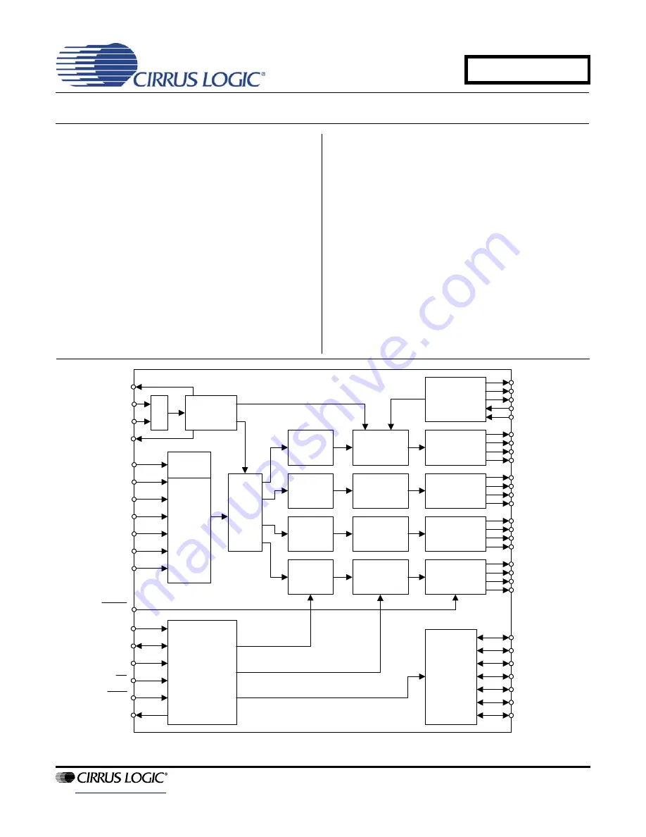
DAI

Serial

Port

XTAL

P

Power

Supply

Rejection

P

SPI/I

2

C Host

Control Port

SCL/CCLK

AD1/CDIN

AD0/CS

RST

INT

PSR_MCLK

PSR_SYNC

PSR_DATA

PWM

Backend

Control/

Status

GPIO4
GPIO5

GPIO0

GPIO1
GPIO2

XTO

XTI

PWMOUTA1-

PWMOUTB1-

P

P

PWMOUTA2-

PWMOUTB2-

P

P

PWMOUTA3-

PWMOUTB3-

MUTE

P

P

PWMOUTA4-

PWMOUTB4-

DAI_MCLK

DAI_SCLK

DAI_LRCK

DAI_SDIN1

DAI_SDIN2

DAI_SDIN3

DAI_SDIN4

Volume

/ Limiter

Multibit

Σ∆

Modulator

PWM

Conversion

PWM

Conversion

PWM

Conversion

PWM

Conversion

Volume

/ Limiter

Multibit

Σ∆

Modulator

Volume

/ Limiter

Multibit

Σ∆

Modulator

Volume

/ Limiter

Multibit

Σ∆

Modulator

PWM

Clock

Control

Auto Fs

Detect

GPIO3

GPIO6

PSR_EN

PSR_RESET

PS_SYNC

SRC

SYS_CLK

SDA/CDOUT

MARCH '06

DS632F1

CS44800

Summary of Contents for CS44800

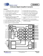
Page 1: ...eps Per Channel Programmable Peak Detect and Limiter SPI and I C Host Control Interfaces Separate 2 5 V to 5 0 V Serial Port and Host Control Port Supplies DAI Serial Port XTAL PWMOUTA1 Power Supply Rejection PWMOUTB1 SPI I2C Host Control Port SCL CCLK AD1 CDIN AD0 CS RST INT PSR_MCLK PSR_SYNC PSR_DATA PWM Backend Control Status GPIO4 GPIO5 GPIO0 GPIO1 GPIO2 XTO XTI PWMOUTA1 PWMOUTB1 PWMOUTA2 PWMO...

Page 2: ...ng analog interference effects which negatively affect system performance The CS44800 integrates on chip digital volume control peak detect with limiter de emphasis and 7 GPIO s allow ing easy interfacing to many commonly available power stages The PWM amplifier can achieve greater than 90 efficiency This efficiency provides for smaller device package less heat sink requirements and smaller power ...

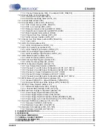
Page 3: ...1 FsIn Domain Clocking 25 4 3 2 FsOut Domain Clocking 25 4 4 FsIn Clock Domain Modules 27 4 4 1 Digital Audio Input Port 27 4 4 2 Auto Rate Detect 31 4 4 3 De Emphasis 31 4 5 FsOut Clock Domain Modules 32 4 5 1 Sample Rate Converter 32 4 5 2 Load Compensation Filter 32 4 5 3 Digital Volume and Mute Control 32 4 5 4 Peak Detect Limiter 33 4 5 5 PWM Engines 33 4 5 6 Interpolation Filter 34 4 5 7 Qua...

Page 4: ... Soft Ramp Down on Interface Error SRD_ERR 56 7 7 5 Soft Ramp Up on Recovered Interface Error SRU_ERR 56 7 7 6 Auto Mute AMUTE 56 7 8 Master Volume Control Integer address 07h 57 7 8 1 Master Volume Control Integer MSTR_IVOL 7 0 57 7 9 Master Volume Control Fraction address 08h 57 7 9 1 Master Volume Control Fraction MSTR_FVOL 1 0 57 7 10 Channel XX Volume Control Integer addresses 09h 10h 59 7 10...

Page 5: ...PWM Configuration Register address 31h 68 7 29 1 Over Sample Rate Selection OSRATE 68 7 29 2 Channels A1 and B1 Output Configuration A1 B1_OUT_CNFG 68 7 29 3 Channels A2 and B2 Output Configuration A2 B2_OUT_CNFG 68 7 29 4 Channel A3 Output Configuration A3_OUT_CNFG 69 7 29 5 Channel B3 Output Configuration B3_OUT_CNFG 69 7 29 6 Channels A4 and B4 Output Configuration A4 B4_OUT_CNFG 69 7 30 PWM Mi...

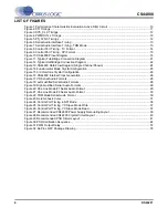
Page 6: ...uration 25 Figure 15 3rd Overtone Crystal Configuration 26 Figure 16 CS44800 Internal Clock Generation 26 Figure 17 I S Serial Audio Formats 28 Figure 18 Left Justified Serial Audio Formats 28 Figure 19 Right Justified Serial Audio Formats 29 Figure 20 One Line Mode 1 Serial Audio Format 29 Figure 21 One Line Mode 2 Serial Audio Format 30 Figure 22 TDM Mode Serial Audio Format 30 Figure 23 De Emph...

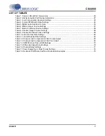
Page 7: ...gs 58 Table 8 Channel Integer Volume Settings 59 Table 9 Channel Fractional Volume Settings 60 Table 10 Limiter Attack Rate Settings 62 Table 11 Limiter Release Rate Settings 62 Table 12 Channel Load Compensation Filter Coarse Adjust 63 Table 13 Channel Load Compensation Filter Fine Adjust 63 Table 14 PWM Minimum Pulse Width Settings 70 Table 15 Differential Signal Delay Settings 70 Table 16 Chann...

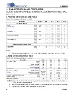
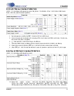
Page 8: ...der voltage is limited by the input current Parameter Symbol Min Typ Max Units DC Power Supply Digital 2 5 V VD 2 37 2 5 2 63 V XTAL Note 1 2 5 V 3 3 V 5 0 V VDX 2 37 3 14 4 75 2 5 3 3 5 0 2 63 3 47 5 25 V V V PWM Interface 3 3 V 5 0 V VDP 3 14 4 75 3 3 5 0 3 47 5 25 V V Serial Audio Interface 2 5 V 3 3 V 5 0 V VLS 2 37 3 14 4 75 2 5 3 3 5 0 2 63 3 47 5 25 V V V Control Interface 2 5 V 3 3 V 5 0 V...

Page 9: ...DOUT AD0 CS AD1 CDIN INT RST MUTE PWM signals include PWMOUTA1 B4 PSR_MCLK PSR_SYNC PSR_DATA PS_SYNC GPIO 6 0 Parameter Symbol Min Typ Max Units Normal Operation Note 4 Power Supply Current Note 5 VD 2 5 V VDX 3 3 V VDP 3 3 V VLS 3 3 V VLC 3 3 V Note 6 ID IDX IDP ILS ILC 150 2 1 2 150 250 mA mA mA µA µA Power Dissipation VD 2 5 V VDX VDP VLS VLC 3 3 V 387 500 mW Power Supply Rejection Ratio Note 7...

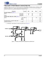
Page 10: ...le 997 Hz 11 Performance characteristics measured using filter shown in Figure 1 Parameter Symbol Min Typ Max Unit Dynamic Performance Note 11 24 Bits A Weighted unweighted 16 Bits unweighted 102 99 108 105 96 dB dB dB Total Harmonic Distortion Noise Note 11 24 Bits 0 dB 20 dB 60 dB THD N 90 77 45 85 dB dB dB Idle Channel Noise Signal to Noise Ratio 110 dB Interchannel Isolation 1 kHz 100 dB PWMOU...

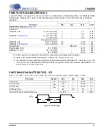
Page 11: ... Fso 4 5 Fsi SWITCHING CHARACTERISTICS XTI VD 2 5 V VDP VLC VLS 3 3 V VDX 2 5 V to 5 0 V Inputs Logic 0 GND Logic 1 VDX Parameter Unit Min Typ Max Digital Filter Response Note 12 Passband OSRATE 0b to 0 01 dB corner to 3 dB corner OSRATE 1b Note 13 to 0 01 dB corner to 3 dB corner 0 0 0 0 1 6 24 0 3 3 44 5 kHz kHz kHz kHz Frequency Response OSRATE 0b 10 Hz to 20 kHz OSRATE 1b Note 13 10 Hz to 40 k...

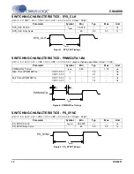
Page 12: ... Cload 20 pF Parameter Symbol Min Typ Max Unit SYS_CLK Period tsclki 18 518 ns SYS_CLK Duty Cycle 45 50 55 Parameter Symbol Min Typ Max Unit PWMOUTxx Period tpwm 2 60 1 18 µs Rise Time of PWMOUTxx VDP 5 0 V VDP 3 3 V tr 1 6 2 1 ns ns Fall Time of PWMOUTxx VDP 5 0 V VDP 3 3 V tf 1 1 1 4 ns ns Parameter Symbol Min Typ Max Unit PS_SYNC Period tpsclki 592 576 ns PS_SYNC Duty Cycle 45 50 55 SYS_CLK tsc...

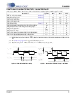
Page 13: ...Cycle Note 16 40 60 DAI_SCLK Duty Cycle 45 55 DAI_LRCK Duty Cycle 45 55 DAI Sample Rate Note 17 Fs 32 192 kHz DAI_SDIN Setup Time Before DAI_SCLK Rising Edge tds 10 ns DAI_SDIN Hold Time After DAI_SCLK Rising Edge tdh 10 ns DAI_SCLK High Time tsckh 20 ns DAI_SCLK Low Time tsckl 20 ns DAI_LRCK Setup Time Before DAI_SCLK Rising Edge tlrcks 25 ns DAI_SCLK Rising Edge Before DAI_LRCK Edge tlrckd 25 ns...

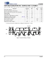
Page 14: ...s tbuf 4 7 µs Start Condition Hold Time prior to first clock pulse thdst 4 0 µs Clock Low time tlow 4 7 µs Clock High Time thigh 4 0 µs Setup Time for Repeated Start Condition tsust 4 7 µs SDA Hold Time from SCL Falling Note 18 thdd 10 ns SDA Setup time to SCL Rising tsud 250 ns Rise Time of SCL and SDA tr 1000 ns Fall Time SCL and SDA tf 300 ns Setup Time for Stop Condition tsusp 4 7 µs t buf t h...

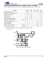
Page 15: ... CS High Time between Transmissions tcsh 1 0 µs CS Falling to CCLK Edge tcss 20 ns CCLK Low Time tscl 66 ns CCLK High Time tsch 66 ns CDIN to CCLK Rising Setup Time tdsu 40 ns CCLK Rising to DATA Hold Time Note 19 tdh 15 ns CCLK Falling to CDOUT Stable tpd 50 ns Rise Time of CDOUT tr1 25 ns Fall Time of CDOUT tf1 25 ns Rise Time of CCLK and CDIN Note 20 tr2 100 ns Fall Time of CCLK and CDIN Note 2...

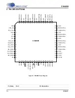
Page 16: ...UTA2 PSR_MCLK PSR_SYNC PSR_DATAL PWMOUTB2 PWMOUTA3 PWMOUTA3 PWMOUTB3 PWMOUTB3 PWMOUTA4 PWMOUTA4 PWMOUTB4 PWMOUTB4 VLC DAI_LRCK DAI_SDIN4 DAI_SDIN1 DAI_SDIN2 DAI_SDIN3 GND VDX GPIO3 GPIO4 GPIO6 GPIO2 VD VDP GND GND VDP SYS_CLK GND PSR_RESET GPIO1 GPIO5 MUTE 1 2 3 4 5 6 7 8 9 10 11 12 13 14 15 16 17 18 19 20 21 22 23 24 25 26 27 28 29 30 31 32 64 63 62 61 60 59 58 57 56 55 54 53 52 51 50 49 48 47 46...

Page 17: ...the logic interface voltage as shown in the Typical Connection Diagram CDOUT is the output data line for the control port interface in SPI mode AD1 CDIN 23 Address Bit 1 I C Serial Control Data SPI Input AD1 is a chip address pin in I C mode CDIN is the input data line for the control port interface in SPI mode AD0 CS 24 Address Bit 0 I C Control Port Chip Select SPI Input AD0 is a chip address pi...

Page 18: ...Power Supply Rejection Sync Clock Input Synchronization signal for external PSR ADC CS4461 PSR_RESET 52 Power Supply Rejection Reset Output The reset pin for the external Power Supply Rejection circuitry PSR_EN 2 Power Supply Rejection Enable Output The enable pin for the external Power Supply Rejection circuitry PWMOUTA1 PWMOUTA1 PWMOUTB1 PWMOUTB1 PWMOUTA2 PWMOUTA2 PWMOUTB2 PWMOUTB2 PWMOUTA3 PWMO...

Page 19: ...DS632F1 19 CS44800 GND 1 4 18 28 36 42 48 53 59 Digital Ground Input Ground reference for digital circuits ...

Page 20: ...ble DAI_SDINx VLS Input 2 5 V and 3 3 5 0 V TTL Compatible DAI_SCLK VLS Input 2 5 V and 3 3 5 0 V TTL Compatible DAI_LRCK VLS Input 2 5 V and 3 3 5 0 V TTL Compatible DAI_MCLK VLS Input 2 5 V and 3 3 5 0 V TTL Compatible SYS_CLK VLS Output 2 5 5 0 V CMOS XTI VDX Input 2 5 V and 3 3 5 0 V TTL Compatible Internal pull down XTO VDX Output GPIOx VDP Input Output 3 3 5 0 V CMOS Open Drain 3 3 5 0 V TTL...

Page 21: ... CONTROL STATUS PWM IN5 OUT5 CONTROL STATUS PWM IN6 OUT6 CONTROL STATUS GPIO3 PWM IN7 OUT7 CONTROL STATUS PWM IN8 OUT8 CONTROL STATUS GPIO5 GPIO6 Optional VD VLC 0 1 µF 2 5 V to 5 0 V SCL CCLK SDA CDOUT AD1 CDIN RST 2 k Ω 2 k Ω Note Resistors are required for I C control port operation See Note DAI_SDIN1 DAI_SDIN3 DAI_SDIN2 DAI_LRCK DAI_SCLK AD0 CS INT Digital Audio Processor Micro Controller DAI_...

Page 22: ...T2 CONTROL STATUS GPIO5 Front Right Surr Left Surr Right Center Subwoofer Rear Left Rear Right GPIO0 GPIO1 VD VLC 0 1 µF 2 5 V to 5 0 V SCL CCLK SDA CDOUT AD1 CDIN RST 2 k Ω 2 k Ω Note Resistors are required for I C control port operation See Note DAI_SDIN1 DAI_SDIN3 DAI_SDIN2 DAI_LRCK DAI_SCLK AD0 CS INT Digital Audio Processor Micro Controller DAI_MCLK VD SYS_CLK MUTE VDX XTAL 24 576 MHz to 54 M...

Page 23: ...vides for a smaller device package less heat sink requirements and smaller power supplies The CS44800 is ideal for audio systems requiring wide dynamic range negligible distortion and low noise such as A V receivers DVD receivers digital speaker and automotive audio systems 4 2 Feature Set Summary Core Features 2 5 V digital core voltage VD VLC voltage pin for host interface logic levels between 2...

Page 24: ...dwidth Power supply clock output PS_SYNC with programmable divider 4 3 Clock Generation The sources for internal clock generation for the PWM processing are as follows FsIn Domain DAI_MCLK minimum 128Fs FsOut Domain XTI XTO Fundamental or 3rd overtone crystal or Clock signal on XTI VDX is used to set logic voltage level DAI_SCLK DAI_SDINx Digital Audio Input Port DAI_MCLK DAI_LRCK Ratio Detect SYS...

Page 25: ... the PDN_XTAL bit in register 02h Mode sample rate range Sample Rate kHz DAI_MCLK MHz DAI_MCLK LRCK Ratio 256x 384x 512x 768x 1024x Single Speed 4 to 50 kHz 32 8 1920 12 2880 16 3840 24 5760 32 7680 44 1 11 2896 16 9344 22 5792 33 8688 45 1584 48 12 2880 18 4320 24 5760 36 8640 49 1520 DAI_MCLK LRCK Ratio 128x 192x 256x 384x 512x Double Speed 50 to 100 kHz 64 8 1920 12 2880 16 3840 24 5760 32 7680...

Page 26: ... provided The clock generation for the CS44800 is shown in the Figure 16 Y1 L1 C3 C1 C2 XTI XTO Figure 15 3rd Overtone Crystal Configuration PWM_MCLK SRC_MCLK XTO XTI MOD_MCLK SYS_CLK PS_SYNC PWM Master Clock Divider System Clock Divider Power Supply Sync Divider PWM Modulator Clock Divider Sample Rate Converter Clock Divider Figure 16 CS44800 Internal Clock Generation ...

Page 27: ... on page 52 The serial audio data is presented in 2 s complement binary form with the MSB first in all formats When operated in One Line Data Mode 6 channels of PWM data are input on DAI_SDIN1 and two addi tional PWM channels on DAI_SDIN4 In TDM mode all 8 channels are multiplexed onto the DAI_SDIN1 data line Table 2 outlines the serial port channel allocations The DAI digital audio serial ports s...

Page 28: ...e of DAI_SCLK For the left justified format the left channel data is presented when DAI_LRCK is high and the right channel data is presented when DAI_LRCK is low Left Channel Right Channel DAI_SDINx 3 2 1 5 4 1 2 3 4 5 3 2 1 5 4 1 2 3 4 MSB MSB LSB LSB DAI_LRCK DAI_SCLK Figure 17 I S Serial Audio Formats I S Mode Data Valid on Rising Edge of DAI_SCLK Bits Sample SCLK Rates 16 32 48 64 128 256 Fs 1...

Page 29: ...iod DAI_LRCK is sam pled as valid on the same clock edge as the most significant bit of the first data sample and must be held high for 64 DAI_SCLK periods Each time slot is 20 bits wide with the valid data sample left justified within the time slot Valid data lengths are 16 18 or 20 bits Valid samples rates for this mode are 32 kHz to 96 kHz Left Channel Right Channel 6 5 4 3 2 1 0 9 8 7 15 14 13...

Page 30: ...a 256 Fs rate DAI_LRCK identifies the start of a new frame and is equal to the sample period DAI_LRCK is sampled as valid on the proceeding clock edge as the most significant bit of the first data sample and must be held valid for at least 1 DAI_SCLK period Each time slot is 32 bits wide with the valid data sample left justified within the time slot Valid data lengths are 16 18 20 24 or 32 bits Va...

Page 31: ... 4 3 De Emphasis The CS44800 includes on chip digital de emphasis filters The de emphasis feature is included to accom modate older audio recordings that utilize pre emphasis equalization as a means of noise reduction Figure 23 shows the de emphasis curve The frequency response of the de emphasis curve will scale pro portionally with changes in sample rate Fs The required de emphasis filter for 32...

Page 32: ...5 kHz with about a 4 dB of gain at around 20 kHz This phe nomenon will cause the system to not meet the frequency response requirements as specified by Dolby Labs By using the programmable 2 pole load compensation filter the overall frequency response of the system can be modified to cut the amount of peaking The 2 poles of the filter are independently configurable and are concatenated to form the...

Page 33: ...nd connects to a driver or a pair of drivers depending on the output configuration Each PWM Engine receives the master clock PWM_MCLK from the Clock Control block and the associated channel data and audio sample timings from the Sample Rate Converter The PWM Configuration Register address 31h on page 68 is used to configure the PWM engines op eration This register controls the parameters of the PW...

Page 34: ...selected switch rate with 64 level resolution The modulator maintains low frequency audio signals allowing the output to reproduce all low frequency audio content down to 0 Hz 4 5 9 PWM Outputs The Modulators outputs are followed by the PWM Configuration block These signals are routed through delay control blocks where they generate two outputs each These final outputs are modulated pulses run nin...

Page 35: ... therefore reduce overall system costs the rejection of harmonic distortion from the power supply and tones coupled onto the power rail is ac complished by the patented power supply rejection realtime feedback By using the CS4461 and associ ated attenuation circuitry the scaled AC and DC components of the power supply rail are fed back into the PWM modulator All delays through the feedback path ha...

Page 36: ...address and must be 1001111 The eighth bit is a read write indi cator R W which should be low to write The next eight bits form the Memory Address Pointer MAP which is set to the address of the register that is to be updated The next eight bits are the data which will be placed into the register designated by the MAP During writes the CDOUT output stays in the Hi Z state It may be externally pulle...

Page 37: ...P will be output Setting the auto incre ment bit in MAP allows successive writes of consecutive registers Each byte is separated by an acknowledge bit The ACK bit is output from the CS44800 after each input byte is read and is input to the CS44800 from the microcontroller after each transmitted byte Autoincrement reads are not supported Since the read operation can not set the MAP an aborted write...

Page 38: ...intended to drive the inter rupt input pin on the host microcontroller The INT pin may be set to be active low active high or active low with an open drain driver This last mode is used for active low wired OR hook ups with multiple pe ripherals connected to the microcontroller interrupt input pin Many conditions can cause an interrupt as listed in the interrupt status register descriptions See In...

Page 39: ...er and ground of the CS44800 The recommended procedure is to place the lowest value capacitor as close as physically possible to each power pin Decoupling capacitors should be as near to the pins of the CS44800 as pos sible with the low value ceramic capacitor being the nearest and mounted on the same side of the board as the CS44800 to minimize inductance effects Figure 27 shows the recommended p...

Page 40: ...ted components for the crystal circuit L1 and C5 are only used for 3rd overtone crystals C3 and C4 should have a C0G NPO dielectric Care should be taken to minimize the distance between the CS44800 XTI XTO pins and C3 Top and bottom ground fill should be used as much as possible around and in between all crystal circuit components to minimize noise Figure 28 Recommended CS44800 Crystal Circuit Lay...

Page 41: ...d input buffer should be placed on the board between the CS44800 and the high voltage power supply The sense point of the high volt age power supply the point at which the input buffer taps off of the high voltage power supply should be close to the middle of the amplifier output channels If the sense point is taken at either end of the amplifier output channels inaccurate reading could occur due ...

Page 42: ... to the bias voltage minimizing the power up transient To prevent an audible transient at the next power on the DC blocking capacitors must fully discharge be fore turning off the power If full discharge does not occur a transient will occur when the audio outputs are initially clamped to GND To prevent transients at power down the user must first mute the outputs When this occurs audio output cea...

Page 43: ...a sequence which will slowly increase the DC voltage from 0V to Vpower 2 across the AC coupling capacitor This will eliminate the instantaneous charge across the capacitor which would have caused an audible pop from the speaker 13 Wait for the ramp up sequence to complete The ramp up function can be configured to cause an interrupt condition when the ramp period has completed This will be indicate...

Page 44: ...ion can be configured to cause an interrupt condition when the ramp period has completed This will be indicated by an active INT signal 5 Once the ramp down sequence has completed set the appropriate GPIO pin or other control signal to power down the power output stage 6 For full bridged power output stage configurations the ramp down sequence is not required Powering down the power output stage w...

Page 45: ...DS632F1 45 CS44800 8 Set the PDN bit to 1 b to put the CS44800 in the power down state ...

Page 46: ...age 57 default 0 0 0 0 0 0 0 0 09h Channel A1 Vol Control Integer CHA1_IVOL7 CHA1_IVOL6 CHA1_IVOL5 CHA1_IVOL4 CHA1_IVOL3 CHA1_IVOL2 CHA1_IVOL1 CHA1_IVOL0 page 59 default 0 0 0 0 0 0 0 0 0Ah Channel B1 Vol Control Integer CHB1_IVOL7 CHB1_IVOL6 CHB1_IVOL5 CHB1_IVOL4 CHB1_IVOL3 CHB1_IVOL2 CHB1_IVOL1 CHB1_IVOL0 page 59 default 0 0 0 0 0 0 0 0 0Bh Channel A2 Vol Control Integer CHA2_IVOL7 CHA2_IVOL6 CH...

Page 47: ...age 62 default 0 0 0 0 0 0 0 0 19h Chnl A1 Comp Filter Fine Adj RESERVED RESERVED CHA1_FINE5 CHA1_FINE4 CHA1_FINE3 CHA1_FINE2 CHA1_FINE1 CHA1_FINE0 page 63 default 0 0 0 0 0 0 0 0 1Ah Chnl B1 Comp Filter Coarse Adj RESERVED RESERVED CHB1_CORS5 CHB1_CORS4 CHB1_CORS3 CHB1_CORS2 CHB1_CORS1 CHB1_CORS0 page 62 default 0 0 0 0 0 0 0 0 1Bh Chnl B1 Comp Filter Fine Adj RESERVED RESERVED CHB1_FINE5 CHB1_FI...

Page 48: ... 0 0 0 0 28h Interrupt Mode Control INT1 INT0 RESERVED RESERVED RESERVED RESERVED RESERVED OVFL_L E page 63 default 0 0 0 0 0 0 0 0 29h Interrupt Mask M_SRC_UNLOCK M_SRC_LOCK M_RMPUP_DONE M_RMPDN_DONE M_MUTE_DONE M_OVFL_INT RESERVED RESERVED page 64 default 0 0 0 0 0 0 0 0 2Ah Interrupt Status SRC_UNLOCK SRC_LOCK RMPUP_DONE RMPDN_DONE MUTE_DONE OVFL_INT GPIO_INT RESERVED page 64 default 0 0 0 0 0 ...

Page 49: ...ED11 DEC_SCALED10 DEC_SCALED09 DEC_SCALED08 page 74 default 0 1 0 1 1 0 0 0 37h PSR_Decimator Scaled DEC_SCALED07 DEC_SCALED06 DEC_SCALED05 DEC_SCALED04 DEC_SCALED03 DEC_SCALED02 DEC_SCALED01 DEC_SCALED00 page 74 default 0 1 1 0 1 0 0 0 38h Reserved RESERVED RESERVED RESERVED RESERVED RESERVED RESERVED RESERVED RESERVED default 0 0 0 0 0 0 0 0 39h Reserved RESERVED RESERVED RESERVED RESERVED RESER...

Page 50: ...ontrol 0 MAP is not incremented automatically 1 Internal MAP is automatically incremented after each read or write 7 1 2 Memory Address Pointer MAPx Default 0000001 Function Memory address pointer MAP Sets the register address that will be read or written by the control port 7 2 CS44800 I D and Revision Register address 01h Read Only 7 2 1 Chip I D Chip_IDx Default 1100 Function I D code for the C...

Page 51: ...a divide by 2 on the XTI clock The state of the MUTE pin will be latched on the rising edge of the RST The MUTE pin can then be used as defined 7 3 3 PWM Master Clock Divider Settings PWM_MCLK_DIV 1 0 Default 00 Function These two bits determine the divider for the XTAL clock signal for generating the PWM_MCLK signal 7 3 4 Power Down XTAL PDN_XTAL Default 0 0 Crystal Oscillator Circuit is running ...

Page 52: ...r down bit defaults to enabled on power up and must be disabled before normal operation can occur 7 4 PWM Channel Power Down Control address 03h 7 4 1 Power Down PWM Channels PDN_PWMB4 PDN_PWMA1 Default 11111111 0 Normal Operation 1 Power down PWM channel Function The specific PWM channel is in the power down state All processing is halted for the specific channel but does not alter the setup or d...

Page 53: ...nabled the output switch rate is divided by 2 25 resulting in a lowered PWM switch rate Care should be taken to ensure that PWM_MCLK 16 the upper frequency limit of the AM tuner used 7 5 3 Freeze Controls FREEZE Default 0 Function This function will freeze the previous output of and allow modifications to be made to the Master Volume Control address 07h 08h Channel XX Volume Control address 09h 12...

Page 54: ...put caused by the DC blocking capacitor When the ramp up down function is disabled in single ended applications there will be an abrupt change in the out put signal Refer to Section 5 1 1 If ramp up or down is not needed as in a full bridge application these bits should be set to 00 If ramp up or down is needed as in a single ended half bridge application these bits must be used in the proper sequ...

Page 55: ...oes not encounter a zero crossing The zero cross function is independently monitored and implemented for each channel Soft Ramp Soft Ramp allows level changes both muting and attenuation to be implemented by incrementally ramp ing in 1 8 dB steps from the current level to the new level at a rate of 1 dB per 8 left right clock periods Soft Ramp on Zero Crossing Soft Ramp and Zero Cross Enable dicta...

Page 56: ...o data from the SRC is no longer consid ered valid and could cause unwanted pops or clicks When this feature is enabled this mute is affected similar to attenuation changes by the Soft and Zero Cross bits SZC 1 0 When disabled an immediate mute is performed on detection of an error Note For best results it is recommended that this bit be used in conjunction with the SRU_ERR bit 7 7 5 Soft Ramp Up ...

Page 57: ... dB incre ments Volume settings are decoded as shown in Table 7 These volume changes are implemented as specified by the Soft and Zero Cross bits SZC 1 0 All volume settings greater than 00011000b are equivalent to 24 dB Binary values for integer and fractional volume settings less than 0 dB are in two s complement form To calculate from a positive decimal integer fraction value to a binary positi...

Page 58: ...r fraction value to a negative decimal do the following 1 Concatenate MSTR_IVOL 7 0 MSTR_FVOL 1 0 to form a 10 bit binary value 2 Perform a 2 s complement conversion on all 10 bits 3 Convert the 10 bit binary number to a decimal value 4 Divide the decimal value by 4 MSTR_IVOL 7 0 MSTR_FVOL 1 0 Volume Setting 0001 1000 00 24 00 dB 0001 0111 10 23 50 dB 0000 0001 11 1 75 dB 0000 0001 00 1 00 dB 0000...

Page 59: ... in the Channel Vol ume Control Integer register and allows global control of the signal levels on all channels in 0 25 dB in crements Volume settings are decoded as shown in Table 7 These volume changes are implemented as specified by the Soft and Zero Cross bits SZC 1 0 All volume settings greater than 00011000b are equivalent to 24 dB Binary values for integer and fractional volume settings les...

Page 60: ...ese bits will invert the signal polarity of their respective channels CHXX_IVOL 7 0 CHXX_FVOL 1 0 Volume Setting 0001 1000 00 24 00 dB 0001 0111 10 23 50 dB 0000 0001 11 1 75 dB 0000 0001 00 1 00 dB 0000 0000 01 0 25 dB 0000 0000 00 0 dB 1111 1111 10 0 50 dB 1111 1111 00 1 00 dB 1111 1110 11 1 25 dB 1111 1101 10 2 50 dB 1000 0010 00 126 00 dB 1000 0001 11 126 25 dB 1000 0001 00 127 00 dB Table 9 C...

Page 61: ...ined by the Limiter At tack Rate register 7 16 Limiter Attack Rate address 16h 7 16 1 Attack Rate ARATE 7 0 Default 00010000 Function The limiter attack rate is user selectable The effective rate is a function of the SRC output sampling fre quency and the value in the Limiter Attack Rate register Rates are calculated using the function RATE 32 value SRC Fs where value is the decimal value in the L...

Page 62: ...e Channel Load Compensation Filter Coarse Adjustment settings control the amount of attenuation of this single pole filter and are used in conjunction with the Fine Adjustment bits to compensate for speaker impedance load variations Each PWM channel is controlled by an associated register The coarse ad justment bits will attenuate the audio response curve according to the table below in 0 1 dB inc...

Page 63: ...20 1 Interrupt Pin Control INT1 INT0 Default 00 00 Active high high output indicates interrupt condition has occurred 01 Active low low output indicates an interrupt condition has occurred 10 Open drain active low Requires an external pull up resistor on the INT pin 11 Reserved Function Determines how the interrupt pin INT will indicate an interrupt condition If any of the mask bits in the Interru...

Page 64: ...are considered edge trigger interrupts The OVFL_INT and GPIO_INT bits will not reset to 0 by reading this register The OVFL_INT bit will be set to 0 by a read to the Channel Over Flow Status address 2Bh Read Only on page 66 only when the in terrupt type is set to edge trigger The GPIO_INT bit will be set to 0 by a read to the GPIO Status Register address 2Fh on page 67 only when the interrupt type...

Page 65: ...e Control Configuration address 06h on page 55 7 22 6 Channel Over Flow Interrupt OVFL_INT Default 0 Function When high indicates that the magnitude of an output sample on one of the channels has exceeded full scale and has been clipped to positive or negative full scale as appropriate This bit is the logical OR of all the bits in the Channel Over Flow Status Register Read the Channel Over Flow St...

Page 66: ... positive or negative full scale as appropriate 7 24 GPIO Pin In Out address 2Ch 7 24 1 GPIO In Out Selection GPIOX_I O Default 0 0 General Purpose Input 1 General Purpose Output Function General Purpose Input The pin is configured as an input General Purpose Output The pin is configured as a general purpose output 7 25 GPIO Pin Polarity Type address 2Dh 7 25 1 GPIO Polarity Type Selection GPIOX_P...

Page 67: ... by reading the GPIO Status Register GPIO inputs configured as level sensitive will not be automatically cleared but will reflect the logic state on the GPIO input The mask bits in the GPIO Interrupt Mask Register have no effect on the operation of these status bits When a GPIO is un masked and enabled to generate an interrupt and is configured as edge trigger a read operation to this register wil...

Page 68: ...r Clock Configuration and Power Control address 02h on page 51 to a 1b Attempts to write this register while the PDN is not set will be ignored 7 29 2 Channels A1 and B1 Output Configuration A1 B1_OUT_CNFG Default 0 0 pwm outputs for both channels A1 and B1 are configured for half bridge operation 1 pwm outputs for both channels A1 and B1 are configured for full bridge operation Function Identifie...

Page 69: ...1 to a 1b Attempts to write this register while the PDN is not set will be ignored 7 29 6 Channels A4 and B4 Output Configuration A4 B4_OUT_CNFG Default 0 0 pwm outputs for both channels A4 and B4 are configured for half bridge operation 1 pwm outputs for both channels A4 and B4 are configured for full bridge operation Function Identifies the output configuration The value selected for this bit is...

Page 70: ...DIFF_DLY 2 0 Default 000 Function The Differential Signal Delay bits allow delay adjustment between each channel s differential signals PWMOUTxx and PWMOUTxx This set of bits control the delay between PWMOUTxx and PW MOUTxx across all active channels The value of this register determines the amount of delay inserted in the output path The effective delay is calculated by multiplying the register v...

Page 71: ...ulated by multiplying the register value by the period of the PWM_MCLK This parameter can only be changed when all mod ulators and associated logic are in the power down state by setting the PDN bit in the register Clock Con figuration and Power Control address 02h on page 51 to a 1b Attempts to write this register while the PDN is not set will be ignored Binary Code Delay Setting multiply by PWM_...

Page 72: ...OUTB2 PWMOUTB2 tchdly tdifdly tdifdly PWMOUTA1 PWMOUTA1 PWMOUTB1 PWMOUTB1 tchdly tdifdly tdifdly PWMOUTA3 PWMOUTA3 PWMOUTB3 PWMOUTB3 tchdly tdifdly tdifdly PWMOUTA4 PWMOUTA4 PWMOUTB4 PWMOUTB4 tchdly tdifdly tdifdly Figure 31 PWM Output Delay ...

Page 73: ...nable Function Enables the on card and internal power supply rejection circuitry This bit will cause the PSR_EN output signal to change logic level A 0 b in this bit will cause the PSR_EN to drive a logic low A 1 b will drive a logic high 7 6 5 4 3 2 1 0 PSR_EN PSR_RESET FEEDBACK_EN RESERVED RESERVED PS_SYNC_DIV2 PS_SYNC_DIV1 PS_SYNC_DIV0 ...

Page 74: ...0 Default 010 Function These bits are used to scale the power supply reading Decimator Outd addresses 3Bh 3Ch 3Dh dur ing the PSR feedback calibration sequence The combination of shift and scale factors DEC_SCALE 18 0 2 DEC_SHIFT 2 0 can be viewed as a floating point coefficient The floating point coefficient will be determined during the PSR feedback calibration sequence See Decimator Scale DEC_S...

Page 75: ...These bits reflect the real time power supply value as measured by the external PSR feedback circuit DEC_OUTD 23 0 has 24 bit precision formatted as signed 2 22 with decimal values from 4 to 4 2 22 Calibration needs to be done to correlate the value of DEC_OUTD 23 0 with the real power supply value A quiet DC power supply without any ripple is treated as 1 0 with DEC_OUTD 23 0 calibrated at 400000...

Page 76: ...reference point The listed minimum and maximum frequencies are guaranteed to be within the Ac from minimum frequency to maxi mum frequency inclusive Interchannel Isolation A measure of crosstalk between the left and right channels Measured for each channel at the converter s output with no signal to the input under test and a full scale signal applied to the other channel Units in deci bels Interc...

Page 77: ...atio of the rms value of the signal to the rms sum of all other spectral components over the specified band width typically 10 Hz to 20 kHz including distortion components Expressed in decibels Measured at 1 and 20 dBFS as suggested in AES17 1991 Annex A 9 REFERENCES 1 Cirrus Logic Audio Quality Measurement Specification Version 1 0 1997 http www cirrus com products papers meas meas html 2 Cirrus ...

Page 78: ... D1 0 390 0 393 BSC 0 398 9 90 10 0 BSC 10 10 E 0 461 0 472 BSC 0 484 11 70 12 0 BSC 12 30 E1 0 390 0 393 BSC 0 398 9 90 10 0 BSC 10 10 e 0 016 0 020 BSC 0 024 0 40 0 50 BSC 0 60 L 0 018 0 024 0 030 0 45 0 60 0 75 0 000 4 7 000 0 00 4 7 00 Nominal pin pitch is 0 50 mmControlling dimension is mm JEDEC Designation MS022 Figure 32 64 Pin LQFP Package Drawing Note See Legend Below 64L LQFP PACKAGE DRA...

Page 79: ...4800 CRD44800 8x50 W Half Bridge Reference Design Board CRD44800 CRD44800 ST FB 8x60 W Full Bridge Reference Design Board CRD44800 ST FB CRD44600 PH FB 2x100 W Full Bridge Reference Design Board CRD44600 PH FB Release Date Changes PP1 May 2005 Updated Features on page 1 Correcte Power Supply Current on page 9 Corrected High Level Input Voltage on page 9 Corrected Low Level Input Voltage on page 9 ...

Page 80: ...r organization with respect to Cirrus integrated circuits or other products of Cirrus This consent does not extend to other copying such as copying for general distribution advertising or promotional purposes or for creating any work for resale CERTAIN APPLICATIONS USING SEMICONDUCTOR PRODUCTS MAY INVOLVE POTENTIAL RISKS OF DEATH PERSONAL INJURY OR SEVERE PROP ERTY OR ENVIRONMENTAL DAMAGE CRITICAL...

Reviews: