DS632F1
39
CS44800
5. POWER SUPPLY, GROUNDING, AND PCB LAYOUT
The CS44800 requires a 2.5 V digital power supply for the core logic. In order to support a number of PWM backend
solutions, separate VDP power pins are provided to condition the interface signals to support up to 5.0 V levels. The
VDP power pins control the voltage levels for all PWM interface signals, PSR interface signals and GPIO for control
and status.
Extensive use of power and ground planes, ground plane fill in unused areas and surface mount decoupling capac-
itors are recommended. It is necessary to decouple the power supply by placing capacitors directly between the
power and ground of the CS44800. The recommended procedure is to place the lowest value capacitor as close as
physically possible to each power pin. Decoupling capacitors should be as near to the pins of the CS44800 as pos-
sible, with the low value ceramic capacitor being the nearest and mounted on the same side of the board as the
CS44800 to minimize inductance effects.
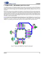
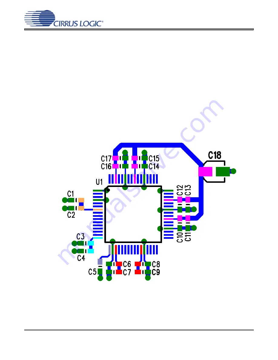
shows the recommended power supply decoupling layout. U1 is the CS44800. C2, C3, C6, C8, C10, C12,
C14, and C16 are 0.01 µF X7R capacitors. These should be placed as close as possible to their respective power
supply pins. C1, C4, C5, C7, C9, C11, C13, C15, and C17 are 0.1 µF X7R capacitors. C18 is a 10 µF electrolytic
capacitor. Top and bottom ground fill should be used as much as possible around all components shown.
Figure 27. Recommended CS44800 Power Supply Decoupling Layout

