42
DS632F1
CS44800
5.1
Reset and Power-Up
Reliable power-up can be accomplished by keeping the device in reset until the power supplies, clocks, and
configuration pins are stable. It is also recommended that the RST pin be activated if the voltage supplies
drop below the recommended operating condition to prevent power-glitch- related issues.
When RST is low, the CS44800 enters a low-power mode and all internal states are reset, including the
control port and registers. When RST is high, the control port becomes operational and the desired settings
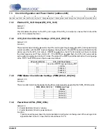
should be loaded into the control registers. Writing a 0 to the PDN bit in the Power Control Register will then
cause the part to leave the low-power state and begin operation.
5.1.1
PWM PopGuard
®
Transient Control
The CS44800 uses PopGuard
®
technology to minimize the effects of output transients during power-up
and power-down. This technique reduces the audio transients commonly produced by half-bridge, single-
supply amplifiers when implemented with external DC-blocking capacitors connected in series with the
audio outputs. Each PWM channel can individually be controlled for ramp-up and ramp-down cycles.
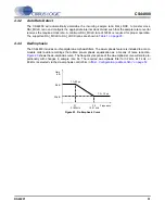
When the device is initially powered-up and configured for ramp-up, the PWMOUTxx outputs are clamped
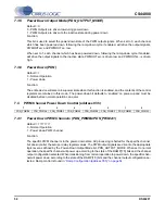
to GND. Following a write of a 0 to the PDN_PWMxx bit in the
PWM Channel Power Down Control (ad-
dress 03h)
register, each output begins to increase the PWM duty cycle toward the bias voltage point. By
a speed set by the RAMP_SPDx bits, the PWMOUTxx outputs will ramp from 0 V (GND) and reach the
bias point (50% PWM duty cycle). This gradual voltage ramping allows time for the external DC-blocking
capacitor to charge to the bias voltage, minimizing the power-up transient.
To prevent an audible transient at the next power-on, the DC-blocking capacitors must fully discharge be-
fore turning off the power. If full discharge does not occur, a transient will occur when the audio outputs
are initially clamped to GND.
To prevent transients at power-down, the user must first mute the outputs. When this occurs, audio output
ceases and the PWM duty cycle is approximately 50% duty cycle, which represents the mute condition.
Once the channels are powered down, the PWMOUTxx outputs slowly decrease the DC offset until it
reaches GND. The time required to reach GND is determined by the RAMP_SPDx bits. This allows the
DC-blocking capacitors to slowly discharge. Once this charge is dissipated, the power to the device may
be turned off, and the system is ready for the next power-on.
5.1.2
Recommended Power-Up Sequence
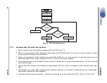
1. Hold RST low until the power supply and clocks are stable. In this state, all control port registers are
reset to the default settings. The PWMOUTxx pins are driven low.
2. The SYS_CLK pin will output a divided-down clock of the signal attached to the XTI pin. If the MUTE
pin is held low, SYS_CLK is equal to the XTI frequency. If the MUTE pin is held high, then SYS_CLK
is equal to the XTI frequency divided by 2.
3. Bring RST high. The device will remain in a low power state and all registers will contain the specified
default value. The logic state of the MUTE pin will be latched and used to specify the clock divider for
SYS_CLK. The control port will be accessible at this time.
4. With the CS44800 in the power-down state, PDN bit is ‘1’b, set up the required PWM configuration
registers and volume control registers. Configure the GPIO pins for normal operation. Do not enable
the power stages at this time.
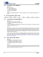
5. Mute all channel outputs by setting the corresponding CHxx_MUTE bits to ‘1’b.

