34
DS632F1
CS44800
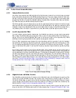
4.5.6
Interpolation Filter
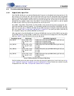
The times 2 (2x) interpolation filter is part of the Quantizer and is used to up sample the data to support
a higher PWM switch rate. The interpolator is controlled by the OSRATE bit in the
“PWM Configuration
Register (address 31h)” on page 68
and employs digital filtering to provide high quality interpolation.
4.5.7
Quantizer
The quantizer takes the input audio data at a typical 384 kHz or 768 kHz rate (depending on whether the
2x Interpolator is on or not) from the Interpolator as input. When PSRR is enabled, the quantizer takes the
input from PSRR Decimator and uses it to correct for power_supply noise. It also provides protection
through min/max pulse limiting hardware to generate outputs that wouldn’t violate minimum pulse widths
required at the PWM drivers. Its stereo outputs are running at the PWM switch rate.
4.5.8
Modulator
Each output from the Quantizer goes to the Modulator. The Modulator takes the parallel input data at a
384 kHz or 768 kHz, depending on the setting of the OSRATE bit, and changes the parallel data to serial,
one-bit outputs. The result is modulated pulses at the selected switch rate with 64 level resolution. The
modulator maintains low frequency audio signals, allowing the output to reproduce all low frequency audio
content down to 0 Hz.
4.5.9
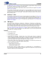
PWM Outputs
The Modulators outputs are followed by the PWM Configuration block. These signals are routed through
delay control blocks where they generate two outputs each. These final outputs are modulated pulses run-
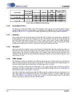
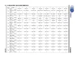
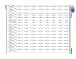
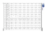
ning at the PWM switch rate as determined by the settings shown in
Table 4
.
Circuitry in the PWM Configuration block guarantees, that no pulses shorter than the minimum pulse are
generated. The minimum pulse width is configured using the MIN_PULSE[4:0] bits in the
“PWM Minimum
Pulse Width Register (address 32h)” on page 69
.
The PWM Configuration block also provides the PWM output signal delay mechanism. Adjusting the out-
puts’ delays allows for managing the switching noise between channels, as well as differential signal
noise. The
“PWMOUT Delay Register (address 33h)” on page 70
specify the delay amount for each PWM
Output. The delay is measured in periods of PWM_MCLK.
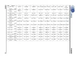
Table 4. Typical PWM Switch Rate Settings
Fsin (kHz)
Fsout (kHz)
using SRC
Quant Level
OSRATE
PWM
Switch Rate
(kHz)
Required XTAL
or SYS_CLK
(MHz)
64
1
384
24.576
64
2
768
49.152
64
1
421.875
27.000
64
2
843.75
54.000
32, 44.1, 48, 88.2, 96,
176.4, 192
384
32, 44.1, 48, 88.2, 96,
176.4, 192
421.875

