DS632F1
41
CS44800
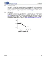
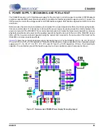
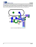
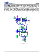
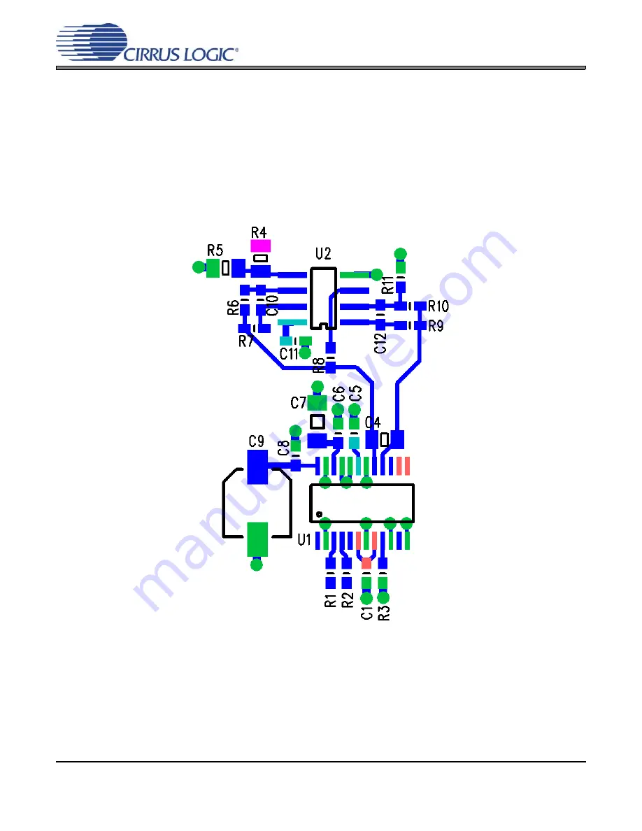
shows the recommended PSR circuit layout. See the CS4461 datasheet for further details on the input
buffer and other associated external components. U1 is the CS4461 and U2 is the input buffer op-amp. All supply
decoupling should be placed as close as possible to their respective power supply pins. C4 should have a C0G
(NPO) dielectric and be placed as close as possible to the CS4461 AIN+/- pins. The CS4461 and input buffer should
be placed on the board between the CS44800 and the high voltage power supply. The sense point of the high volt-
age power supply (the point at which the input buffer taps off of the high voltage power supply) should be close to
the middle of the amplifier output channels. If the sense point is taken at either end of the amplifier output channels,
inaccurate reading could occur due to localized channel disturbances causing noise on the high voltage power sup-
ply. Optimally, the high voltage power connector should also be placed in the middle of the amplifier output channels
Figure 29. Recommended PSR Circuit Layout

