


PMA_CHR_CD40199_R01_allPIXA_SWIR_GigE_User_Manual.docx
23
5.1.3.3 I/O Voltage requirements
Voltage
Description
+0 to + 5.0 VDC
Represents the recommended I/O operating voltage.
+0 to + 0.8 VDC
The voltage value indicates a logical state of 0.
> +0.8 to +2.0 VDC
Defines the value interval for the transition threshold.
No logical state is defined in this region.
> +2.0 VDC
The voltage value indicates a logical state of 1.
+6.0 VDC
Defines the absolute maximum voltage value. Do not
exceeded absolute maximum value.
Never exceeded absolute maximum value for the I/O voltage as this will
result in damage to the camera and/or the surrounding environment.
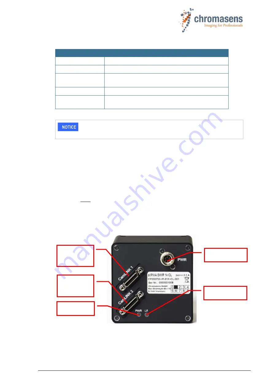
5.2 Connectors and LEDs of the camera with Camera Link
interface
On the backside of the camera, you find the following interfaces:
◼
Two Camera Link MDR connectors for image data transfer and communication between the
allPIXA SWIR camera and the image processing computer. Only CamLINK 1 is required.
◼
A power connection (Hirose HR10A-7P-6S(73) male) for power supply. For more information,
see section 5.1.1.
◼
A power LED, which indicates whether the allPIXA SWIR camera is connected to the power
supply.
◼
A status LED, which blinks as soon as the camera firmware has booted successfully.
Figure 10: Connections and LEDs of the allPIXA SWIR Camera Link camera
5.3 Using an encoder or external triggers
Acquisition Start
,
Frame Start
and
Line Start
can optionally be triggered by (synchronized
with) external trigger sources like rotary encoders or light barriers.
Power
LED
Camera Link
interface 2
(not required)
Status LED
Camera Link
interface 1
(required)
Power LED
Power connector


