


© Cobham Gaisler AB
Kungsgatan 12 | SE-411 19 Goteborg | Sweden
+46 31 7758650 | www.caes.com/gaisler
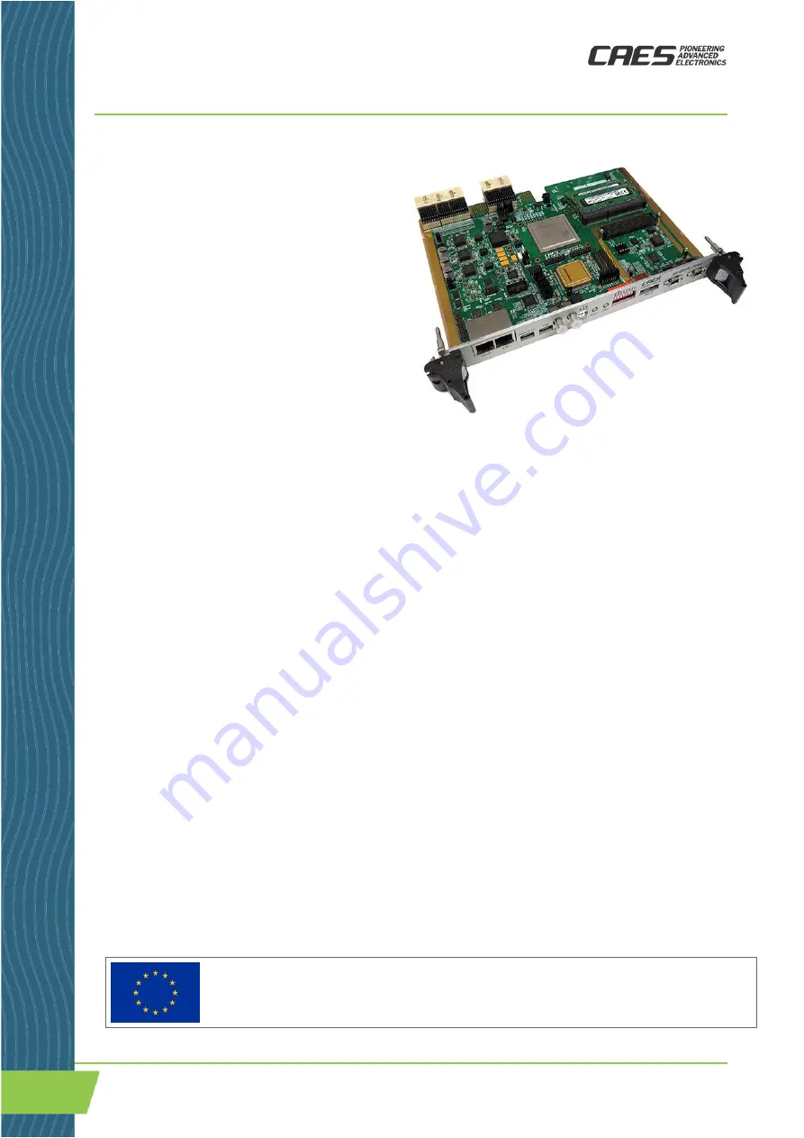
GR-CPCIS-XCKU Development Board
GR-CPCIS-XCKU
GR-CPCIS-XCKU-DSUM
Feb 2022, Version 1.2
Baseline features
The GR-CPCIS-XCKU is an FPGA development
board. Its cutting-edge technology allows the
development of next-generation system on
chips and its interfaces are particularly suited
to emulate space applications.
This board implements a Xilinx Ultrascale
FPGA, in a 1517 ball-grid-array package. The
board was initially designed to use a XCKU060
sized device but is compatible with larger
devices of the same series with the same
footprint.
Optionally, the board also features a GR716
rad-hard microcontroller which can act as the
FPGA supervisor for scrubbing and
programming.
The GR-CPCIS-XCKU is a 1 slot, 6U high
board with a CPCI-S backplane format, and
can be used stand alone on the bench top, or
installed in a CPCI-Serial rack
The GR-CPCIS-XCKU includes:
•
Xilinx XCKU, in 1517 pin FCBGA package.
•
GR716 microcontroller. - Optional
•
FPGA interface to DDR3 SDRAM via two
SODIMM connectors.
•
SPI flash for FPGA configuration (512
Mbit), for GR716 boot (256 Mbit), and for
data (256 Mbit). The FPGA has also access
to two NVM: 512 Mbit SPI and Parallel
Flash memory (40 bit wide)
•
FMC Mezzanine expansion connector.
•
Scrubbing interface for FPGA. Available
also without the GR716.
•
2×10 connector to interface with a GR-
ACC-6U_6UART breakout board providing
access to 6 UARTS (or 16 GPIOs).
Front Panel interfaces
•
2x RJ45 to FPGA via magnetics and Gbit
Ethernet transceivers. RGMII interface to
FPGA
•
1x eSATA for SpaceFibre to FPGA via CML
redriver.
•
2x MDM9 for SpaceWire via LVDS
transceivers/repeaters to FPGA.
•
Status LEDs, push-buttons and switches
•
2xSMA or 2xSMB for PPS time distribution to
FPGA.
•
2xUSB ports for:
o
JTAG access to FPGA and FMC
(separate chains)
o
GR716 debug UART and two FPGA
UARTs
Backplane interfaces
•
8 x SpaceFibre for full-mesh interconnect
using FPGA GTH banks
•
8 x SpaceWire for dual-star interconnect
•
Dual-redundant CAN-bus to FPGA and/or
GR716 via two or four transceivers
•
SGPIO and I2C connected to FPGA with
jumper-configurable pull-ups
•
12V supply from backplane that can be turned
off by the external input PS_ON#
•
Other utility signals connected to the FPGA
This board design is part of a project that has received funding from the
European
Union's Horizon 2020 research and innovation programme
under Grant Agree-
ment No 869945.
Data Shee
t & User M
anual
Fe
b
2022