11
ATAB5749 [APPLICATION NOTE]
9138B–AUTO–07/15
●
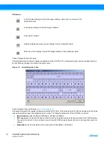
FSK Shift:
the frequency deviation of the FSK modulation can be set with this menu by determining the value of the
FSEP register.
●
Output Power:
this menus sets the transmit power of the IC for 50
matching. The value can be programmed from
–0.5dBm to 12.5dBm in 1dB step. The
green check mark
in the drop down menu shows the default setting of the
demo board, the 12.5dBm transmit power output at 50
matching. The matching of the loop antenna is optimized for
the 12.5dBm transmit power. The power setting can be programmed as described in the datasheet with the constraint
that the default matching of the loop antenna would not be the optimum matching for other power setting. The power
setting with the suboptimal matching due to the default matching is marked with the
yellow check mark
. The
red cross
in the drop down menu shows the values that are not allowed.
●
Clock Only Mode:
in this menu “Clock Only Mode” or “Normal Mode” can be chosen. With Clock Only Mode, the
ATA5749 generates a clock signal based on the crystal frequency for the microcontroller and no transmission will be
performed.
●
CLK Output:
this menu sets the clock output frequency (f
CLK
) of the ATA5749 based on the crystal frequency (f
XTO
).
ATA5749 is able to generate two different clock frequencies, the f
XTO/8
or f
XTO/4
. As the crystal frequency of the
ATAB5749 is 13.0MHz, a 3.25MHz or 1.625MHz clock frequency can be generated.
●
Clock On:
this menu allows the user to switch on and off the clock output of the ATA5749. Under normal operation of
the ATAB5749, the clock output of the transmitter must be always switched on because the data generated by the
microprocessor is derived from this clock frequency. Only during the transmitting of the continuous carrier, can the
clock frequency can be negligible.
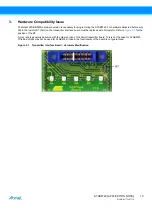
shows the warning displayed by the software if the clock output must be
deactivated.
Figure 2-8.
Control Register Value
Figure 2-9.
Error Code when Clock Output of the ATAB5749 Must be Deactivated


