ATAB5749 [APPLICATION NOTE]
9138B–AUTO–07/15
6
1.2
Software
The board ATAB5749 is be delivered with default settings as detailed in the
below.
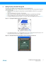
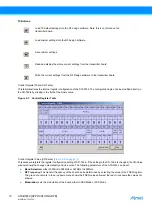
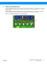
In order to use the ATAB5749 board, an additional board as well as the RF Design Kit software is needed. Either the
ATAB-RFMB or ATAB-STK-F is used as a microprocessor board interfacing the RF Design Kit software and the transmitter
board. For further information about the hardware refer to the application notes “ant_hd-rf-desing-kit_041105_sec.pdf” and
“ant_hd-flamingo_181105_sec.pdf”.
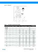
L1
1
x
27nH
2%
0603CS
0603
Coilcraft
®
1
x
47nH
2%
0603CS
0603
Coilcraft
L2
1
x
12nH
2%
0603CS
0603
Coilcraft
1
x
27nH
2%
0603CS
0603
Coilcraft
Q1
1
x
x
13MHz
5032//3225
KSS
®
U1
1
x
x
ATA5749
TSSOP10
Atmel
U2
1
x
x
ATmega88
MLF32
Atmel
D1, D2
2
x
x
TLMD3100
P-LCC-2
(sizeB)
Vishay
®
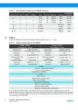
Table 1-1.
Bill of Material of the Demo Board ATAB5749 (Continued)
Components
Pieces
315MHz
433MHz
Value
Tolerance
Material
Housing
Manufacturer/
Distributor
Table 1-2.
Software Default Settings of the ATAB5749
ATA5749 - 433MHZ
ATA5749 - 315MHZ
Control Register - Values
Control Register - Values
Band selection:
367MHz to 450MHz
Band selection:
300MHz to 368MHz
RF frequency:
433.92MHz (FREQ = 14353)
RF frequency:
315MHz (FREQ = 3741)
Modulation:
FSK
Modulation:
FSK
FSK shift:
±30kHz (FSEP = 75)
FSK shift:
±30kHz (FSEP = 75)
Output power (with 50
matching):
+12.5dBm (PWR = 15)
Output power (with 50
matching):
+12.5dBm (PWR = 15)
Clock Only Mode:
Normal Mode
Clock Only Mode:
Normal Mode
CLK output:
3.25MHz (f
CLK
= f
XTO
/4)
CLK output:
3.25MHz (f
CLK
= f
XTO
/4)
Clock on:
Clock port is ON
Clock on:
Clock port is ON
Telegram
Data rate: 1,000Kbit/s (Manchester)
Preburst: 24 bits (24.000 ms)
Testword (Hex): F09AF09A
Pattern
TStep: 90.91µs
Pattern Length: 24 bit (2.1818ms)
Pattern (Hex): 0x5555h
Programmable Push Buttons
Button S1: Continuous telegram
Button S2: Single telegram
Button S3: Continuous carrier (unmodulated)

