


reducing and/or eliminating wait state (IOCHRDY) conditions.
• All status registers are properly latched as well to prevent change in values during a bus read cycle.
• I/O Read line is digitally filtered to support noisy bus problems and eliminate the possibility of dropped analog input data.
• Indexed register array banked over the 8254 registers. This opens the door for many new functions as described above.
• Moving average filter has been corrected to present channel data in the proper order.
Update as of January 15, 2008 (Revision 090115H)
• 8254 Counter/Timer is also available within the indexed register set. This allows software access to all registers when the
indexed register set is enabled.
Please note that all of the new registers are designed such that if they are not configured, everything defaults to the classic
modes of operation. Thus, existing software will function without modification. Writing values to the new registers enhances
operations.
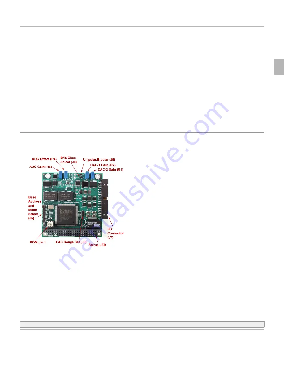
3.2
Photo
3.2 Photo
STX104 Reference Manual
Copyright © 2009 by
Apex Embedded Systems
. All rights reserved.
Thursday, October 08, 2009
7
3


