


UG-1882
Rev. 0 | Page 14 of 28
EVALUATION SOFTWARE OPERATION
LAUNCHING THE AD4696 ACE PLUGIN
After the EVAL-AD4696FMCZ and
are correctly
connected to the PC as described in the Evaluation Hardware
Setup Procedure section, launch the
described in the following steps.
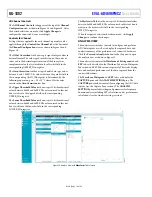
1.
From the
Start
menu, select
All Programs > Analog Devices
> ACE > ACE.exe
, which opens the window shown in
2.
Double click the
AD4696 Evaluation Board
icon in the
Attached Hardware
section in the ACE
Start
window to
evaluation board view (see Figure 13).
3.
Double click the
AD4696
chip icon to display the AD4696
chip view (see Figure 14).
DESCRIPTION OF CHIP VIEW
After completing the steps in the Software Installation section
and the Launching the AD4696 ACE Plugin section, the
AD4696 chip view is displayed. The AD4696 chip view allows
the user to configure the most commonly used AD4696 device
features and for navigating to the other plugin views described
throughout the Evaluation Software Operation section.
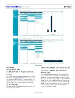
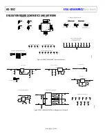
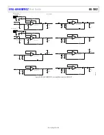
Block Diagram Configuration Menus
The AD4696 chip view includes a block diagram representation
of the AD4696 with controls for configuring the connected
device on the EVAL-AD4696FMCZ. Block icons that are dark
blue are programmable blocks. Clicking a dark blue block icon
opens a pop up window with controls for configuring several
AD4696 device features and settings.
Modifying the controls in any block icon automatically updates
the relevant registers and bit fields in the memory map view.
The controls in each block icon also update if their corresponding
registers and bit fields are modified directly in the memory map
view.
After selecting the desired device configuration settings in the
block icons in the chip view, click the
Apply Changes
button to
apply the new settings to the connected hardware.
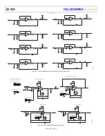
Plugin View Navigation Buttons
On the chip view are the following view navigation buttons (see
Figure 15):
•
Configure Sequence
•
Configure Channels
•
Proceed to Analysis
•
Proceed to Memory Map
The
Configure Sequence
button opens either the
Standard
Sequencer
view or the
Advanced Sequencer
view, depending
on which sequencer mode is selected in the software memory map
(see the Description of the Standard Sequencer View section
and the Description of the Advanced Sequencer View section).
The
Configure Channels
button opens the
Channel
Configuration
view (see the Channel Configuration View
section).
The
Proceed to Analysis
button opens the
AD4696 Analysis
view (see the Analysis View section).
The
Proceed to Memory Map
button opens the
AD4696
Memory Map
view (see the Memory Map View section).
Memory Map Side-by-Side View
Clicking the
Memory Map Side-By-Side
button displays the
memory map view in a window beside the chip view. Displaying
the chip view and memory map view side-by-side allows the user
to observe which bit field and register settings in the AD4696
memory map correspond with GUI controls in the chip view.
SEQUENCER CONFIGURATION VIEWS
The AD4696 ACE plugin includes two sequencer configuration
views that streamline the setup of channel sequences for the
AD4696 standard sequencer and advanced sequencer. The
sequencer configuration views are a GUI representation of the
multiplexer channel sequence settings programmed into the
AD4696 via the device memory map. See the AD4696 data
sheet for a detailed description of the standard sequencer and
advanced sequencer.
The sequencer configuration views include the following:
•
Standard sequencer view
•
Advanced sequencer view
Accessing the Sequencer Configuration Views
The standard sequencer view and the advanced sequencer view
can be accessed from either the chip view or the analysis view.
In the chip view, press the
Configure Sequence
button to
display either the standard sequencer view or the advanced
sequencer view (see the Plugin View Navigation Buttons section).
In the analysis view, select either the standard sequencer or
advanced sequencer using the
Sequencer Mode
dropdown box
and click the
Go To Sequencer
button to display the selected
sequencer configuration view (see the Analysis View section).
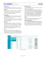
Description of the Standard Sequencer View
The standard sequencer view appears as shown in Figure 16.
Select the list of channels that are to be a part of the sequence
using the
Channel Enable
checkboxes, and click
Apply
Changes
to configure the connected device accordingly.
The
Channel Sample Rates
indicators display the effective
sample rates computed for each channel enabled in the standard
sequencer via the
Channel Enable
checkboxes, where FSR
refers to the sample rate setting stored in the
Throughput
(kSPS)
control in the analysis view (see Figure 20).


