Chapter 1: Nios II Hardware Development
1–29
Creating the Design Example
May 2011
Altera Corporation
Nios II Hardware Development Tutorial
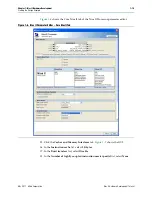
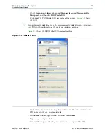
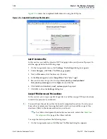
shows the
Unused Pins
page of the
Device and Pin Options
dialog box.
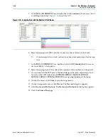
14. In the
Reserve all unused pins
list, select
As input tri-stated with weak pull-up
.
With this setting, all unused I/O pins on the FPGA enter a high-impedance state
after power-up.
c
Unused pins are set as input tri-stated with weak pull-up to remove contention which
might damage the board. Depending on the board, you might have to make more
assignments for the project to function correctly. You can damage the board if you fail
to account for the board design. Consult with the maker of the board for specific
contention information.
15. Click
OK
to close the
Device and Pin Options
dialog box.
16. Click
OK
to close the
Device
dialog box.
f
For more information about making assignments in the Quartus II software, refer to
the
Volume 2: Design Implementation and Optimization
of the
Quartus II Handbook
.
Compile the Quartus II Project and Verify Timing
At this point you are ready to compile the Quartus II project and verify that the
resulting design meets timing requirements.
You must compile the hardware design to create a
.sof
that you can download to the
board. After the compilation completes, you must analyze the timing performance of
the FPGA design to verify that the design will work in hardware.
Figure 1–17. The Unused Pins Page of the Device and Pin Options Dialog Box

