1–12
Chapter 1: Nios II Hardware Development
Creating the Design Example
Nios II Hardware Development Tutorial
May 2011
Altera Corporation
Perform the following steps:
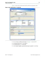
1. On the
Project Settings
tab, select the
Device Family
that matches the Altera
FPGA you are targeting.
1
If a warning appears stating the selected device family does not match the
Quartus project settings, ignore the warning. You specify the device in the
Quartus project settings later in this tutorial.
2. In the documentation for your board, look up the clock frequency of the oscillator
that drives the FPGA.
f
For Altera development board reference manuals, refer to the
page of the Altera website.
3. On the
Clock Settings
tab, double-click the clock frequency in the
MHz
column
for
clk_0
.
clk_0
is the default clock input name for the Qsys system. The
frequency you specify for
clk_0
must match the oscillator that drives the FPGA.
4. Type the clock frequency and press Enter.
Next, you begin to add hardware components to the Qsys system. As you add each
component, you configure it appropriately to match the design specifications.
Add the On-Chip Memory
Processor systems require at least one memory for data and instructions. This design
example uses one 20 KB on-chip memory for both data and instructions. To add the
memory, perform the following steps:
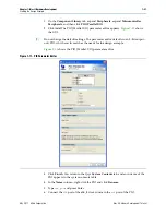
1. On the
Component Library
tab (to the left of the
System Contents
tab), expand
Memories and Memory Controllers
, expand
On-Chip
, and then click
On-Chip
Memory (RAM or ROM).
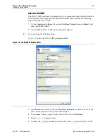
2. Click
Add
. The On-Chip Memory (RAM or ROM) parameter editor appears.
shows the GUI.
3. In the
Block type
list, select
Auto
.
4. In the
Total memory size
box, type
20480
to specify a memory size of 20 KB.
1
Do not change any of the other default settings.


