


ZYNQ FPGA Development Board AX7350B User Manual
25 / 46
Amazon Store: https://www.amazon.com/alinx
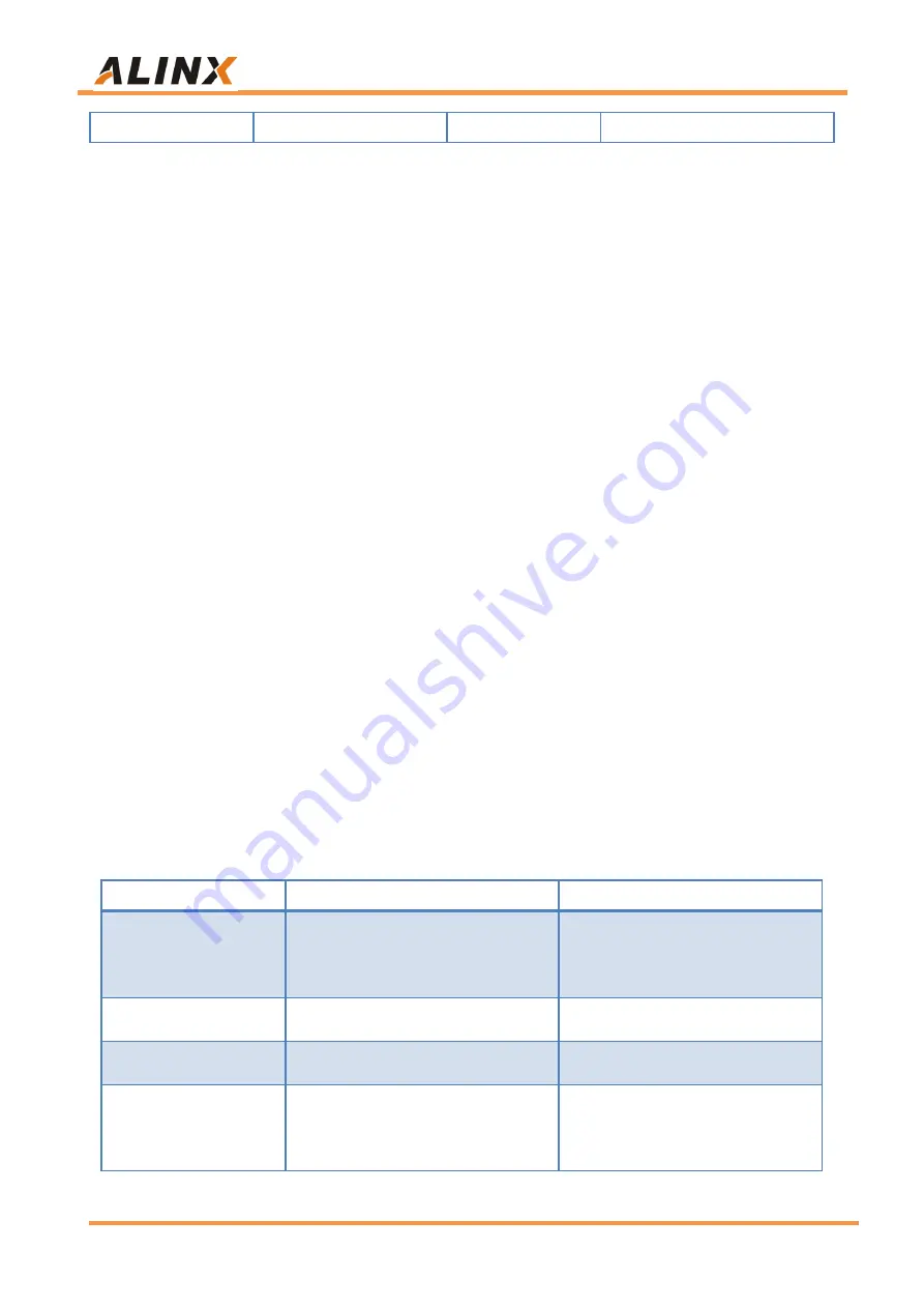
UART_TXD
PS_MIO12_500
A23
Uart data output
Part 8: Gigabit Ethernet Interface
The AX7350B FPGA development board has two Gigabit Ethernet
interfaces, one of which is the connected PS system end, and the other one is
connected to the logical IO port of the PL. The Gigabit Ethernet interface
connected to the PL side needs to be mounted to the ZXIQ AXI bus system by
calling the IP.
The Ethernet chip uses JLSemi JL2121-N040I Industrial Ethernet GPHY
chip to provide network communication services to users. The Ethernet PHY
chip on the PS side is connected to the GPIO interface of the PSNK501 of the
PS side of ZYNQ. The Ethernet PHY chip on the PL side is connected to the IO
of the BANK35. The JL2121 chip supports 10/100/1000 Mbps network
transmission rate and communicates with the MAC layer of the Zynq7000
system through the RGMII interface. JL2121 supports MDI/MDX adaptation,
various speed adaptation, Master/Slave adaptation, and supports MDIO bus for
PHY register management.
The JL2121 power-on will detect the level status of some specific IOs to
determine their working mode. Table 8-1 describes the default setup
information after the GPHY chip is powered up.
。
Configuration Pin
Instructions
Configuration value
RXD3_ADR0
RXC_ADR1
RXCTL_ADR2
MDIO/MDC
Mode
PHY
address
PHY Address 001
RXD1_TXDLY
TX
clock 2ns delay
delay
RXD0_RXDLY
RX clock 2ns delay
delay
RXD3_ADR0
RXC_ADR1
RXCTL_ADR2
MDIO/MDC
Mode
PHY
address
PHY Address 001