24
GR-UT699 Development Board
User Manual
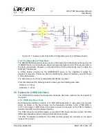
generating a system reset in the event of a software malfunction or crash.
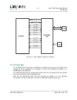
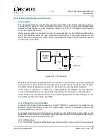
On this development board the
WDOGN
signal is connected as shown in the Figure 2-15 to
the Processor Supervisory circuit.
To utilise the Watchdog feature, it is necessary to appropriately set-up and enable the
Watchdog timer. Please consult the
UT699
data sheet (RD-3) for the correct register
locations and details.
Also, to allow the
WDOGN
signal to generate a system reset it is necessary to install the
Jumper JP1 pins 7-8 (see Figure 2-15).
For software development it is often convenient or necessary to disable the Watchdog
triggering in order to be able to easily debug without interference from the Watchdog
operation. In this case, the Jumper JP1 7-8 should be in the
removed
. When the watchdog
triggers, the Watchdog LED's will illuminate, but a system reset will not occur.
2.12.4 JTAG interface
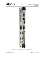
A 14 pin connector on the front panel provides the possibility to connect to the JTAG signals
and JTAG chain of the
UT699
ASIC.
This interface allows DSU Debug over the JTAG interface to be performed.
2.12.5 Mezzanine/Memory Expansion
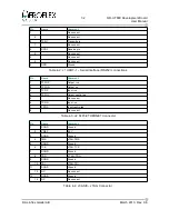
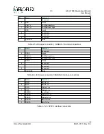
Two connectors, J9 and J11, are provided on the board which give access to the memory
bus signals of the UT699 processor. The signals which are made available on these
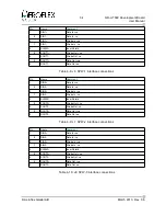
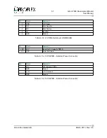
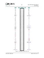
connectors are listed in Table 4-11 and Table 4-13 respectively.
This can allow users to implement either memory expansion on a mezzanine, or by including
the appropriate decoding logic on the mezzanine board, to implement peripheral circuits
mapped in the address range of the I/O space of the UT699 processor.
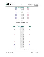
Figure 2-16, shows the pin numbering scheme as implemented on the GR-UT699 Board.
© Aeroflex Gaisler AB
March 2013, Rev. 0.6
Figure 2-15: Watchdog configuration
JUMPER
JP1D
7-8
UT699RH
ASIC
POWER-ON
RESET
CIRCUIT
RESETN
WDOGN
RSTIN_N
FRONT
PANEL
LED
BOARD
MOUNTED
LED


