12
GR-UT699 Development Board
User Manual
2.3.1 SRAM
The
GR-UT699
board is laid out with two SRAM memory banks but only has one bank
mounted as standard. Each bank is made up of five
CY7C1069AV33
. These devices are
16Mbit (2Mbyte x 8 bit devices with 10 or 12 ns access times.
The five devices provide (32 + 8) bit wide SRAM memory paths allowing EDAC operation.
These memory banks are mapped as RAMBANK0 and RAMBANK1.
In case the user wishes to disable the on board memory, this can be done by removing the
jumpers JP5 on the PCB.
2.3.2 FLASH
The
GR-UT699
board has mounted as standard one FLASH memory bank, made up of two
Intel
JS28F640J3
FLASH devices
.
These devices are 64Mbit (8Mbyte x 16 bit devices),
typically with 90ns access times. The data bus width to the Flash memory is 32 bits wide.
Note that, the PROM width and PROM EDAC conditions are set by the state of the
GPIO[2..0] pins at power up of the Processor. Therefore the GPIO[2..0] DIP switches on the
PCB must be appropriately set for the correct operation of the PROM memory at start up of
the processor. For information on the GPIO[2..0] settings refer to the Memory Configuration
documentation in the Leon3 User Manual, or RD-3.
2.3.3 EEPROM
The
GR-UT699
board additionally has a DIP32 socket suitable for mounting an EEPROM
device. The data bus width to the EEPROM device is 8 bits wide.
This socket is suitable for mounting an EEPROM device of the type
AT28LV010,
or
compatible, in DIP32 package. The
AT28LV010
is an ATMEL EEPROM, of 1Mbit capacity
organised as 128kByte x 8 bits.
Jumpers are provided to enable the user to select either the FLASH PROM device or the
EEPROM to operate as the
ROMBANK0
device which appears at the initial memory location
of 0x00000000.
2.3.4 MEMORY EXPANSION CONNECTOR
Access to the memory signals is provided by the connectors J9 and J11. This enables uses
to conceive their own mezzanine boards and functions. Please see section.2.12.5
2.4 CAN Interface
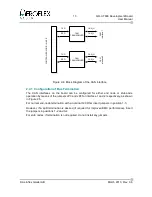
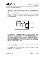
The board provides the electrical interfaces for two CAN bus interfaces, as represented in
the block diagram, Figure 2-4.
The CAN bus transceiver IC's on this board are
SN65HVD230
devices from Texas
Instruments which operate from a 3.3V power supply.
The connector interfaces are male DSUB-9 connectors adhering to the standard pin-out for
this type of interface (ref. Table 4-6 And Table 4-5).
© Aeroflex Gaisler AB
March 2013, Rev. 0.6


