11
GR-UT699 Development Board
User Manual
2.3 Memory
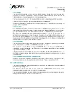
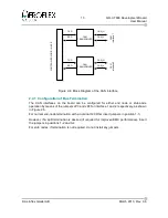
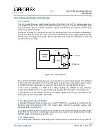
The memory configuration installed on the board is shown in the figure below comprising of:
•
80Mbit of SRAM memory, organised as 1 banks x 2Mword x 40 bits wide
(a second SRAM bank can be installed on the PCB, but is not fitted as standard)
•
128Mbit of Flash PROM, organised as 1 bank x 4 Mword x 32 bits wide)
•
DIL 32 pin socket to allow 1Mbit of EEPROM organised as 1 bank x 128kByte x 8
bits wide) to be installed
Additionally, in order to allow users to install alternative memory configurations or devices, all
the signals of the memory interface are connected to memory expansion connectors. The
expansion connectors allow mezzanine boards to be added similar to those developed for
the
existing
GR-CPCI
development boards.
© Aeroflex Gaisler AB
March 2013, Rev. 0.6
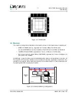
Figure 2-2: UT699 ASIC
Figure 2-3: On-Board Memory Configuration
SRAM
SRAM
UT699RH
ASIC
UT699RH
ASIC
SRAM
SRAM
SRAM
32
ADDR
BANK0
DATA
FLASH
FLASH
8
EEPROM
EEPROM
SRAM
(32+8)
SRAM
SRAM
SRAM
SRAM
SRAM
SRAM
BANK1
M
E
M
O
R
Y
E
X
P
A
N
S
IO
N
C
O
N
N
E
C
T
O
R
CONTROL
R
O
M
S
N
0
R
A
M
S
N
0
R
A
M
S
N
1


