


56 / 246
56 / 246
AC30M1x64/1x32
ABOV Semiconductor
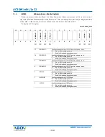
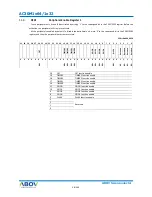
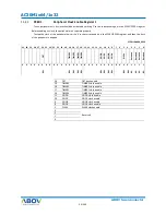
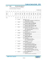
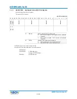
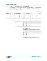
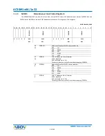
VDCCON
VDC Control Register
1.5.18
On chip VDC control register. VDCTRIM is used for the trim value of VDC output. To modify VDCTRIM bit, VDCTE should
be write ‘1’ simultaneously. VDCWDLY value can be written with writing ‘1’ to VDCDE bit simultaneously. To change
VDCCON register value, it has to enter TRIM mode.
VDCCON=0x4000_0064
31 30 29 28 27 26 25 24 23 22 21 20 19 18 17 16 15 14 13 12 11 10 9
8
7
6
5
4
3
2
1
0
V
D
C
M
E
R
e
se
rv
e
d
ST
O
P
SE
L
R
e
se
rv
e
d
R
e
se
rv
e
d
V
D
C
D
E
V
D
C
W
D
LY
0
0
0
0x04
WO
WO
WO
WO
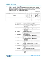
31
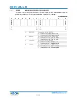
VDCME
VDCMODE value write enable. Write only with VDCMODE value.
0
VDCMODE field is not updated by writing
1
VDCMODE filed can be updated by writing
25
STOPSEL
STOP MODE Select bit.
0
VDC STOP MODE 1
1
VDC STOP MODE 2
8
VDCDE
VDCWDLY value write enable. Write only with VDCWDLY value
0
VDCWDLY Write disable
1
VDCWDLY Write Enable
3
0
VDCWDLY
VDC warm-up delay count value.
When SCU is waked up from power down mode, the warm-up
delay is inserted for VDC output being stabilized.
The amount of delay can be defined with this register value 4 :
2msec
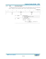
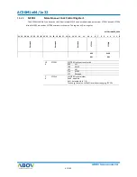
CAUTION!!) you must not set the reserved bit field.
Note) how to enter TRIM mode to change VDCCON value.
FM->MR=0xa5;
FM->MR=0x5a;
// TRIM mode enter
SCU->VDCCON = (1UL<<31) | (1UL<<25); // set VDC STOP MODE 2
FM->MR=0; // TRIM mode exit
Summary of Contents for AC30M1x32
Page 3: ...3 246 ABOV Semiconductor INTRODUCTION SECTION 1 INTRODUCTION ...
Page 4: ...4 246 4 246 AC30M1x64 1x32 ABOV Semiconductor OVERVIEW CHAPTER 1 ...
Page 18: ...18 246 18 246 ABOV Semiconductor AC30M1x64 1x32 CPU CHAPTER 2 ...
Page 22: ...22 246 22 246 ABOV Semiconductor AC30M1x64 1x32 Boot Mode CHAPTER 3 ...
Page 26: ...26 246 26 246 ABOV Semiconductor AC30M1x64 1x32 SECTION 2 PERIPHERALS ...
Page 27: ...27 246 ABOV Semiconductor System Control Unit SCU SYSTEM CONTROL UNIT SCU CHAPTER 1 ...
Page 69: ...69 246 ABOV Semiconductor Port Control Unit PCU PORT CONTROL UNIT PCU CHAPTER 2 ...
Page 85: ...85 246 ABOV Semiconductor General Purpose I O GPIO GENERAL PURPOSE I O GPIO CHAPTER 3 ...
Page 92: ...92 246 92 246 AC30M1x64 1x32 ABOV Semiconductor FLASH MEMORY CONTROLLER CHAPTER 4 ...
Page 105: ...105 246 ABOV Semiconductor Internal SRAM INTERNAL SRAM CHAPTER 5 ...
Page 107: ...107 246 ABOV Semiconductor Watch Dog Timer WATCH DOG TIMER WDT CHAPTER 6 ...
Page 113: ...113 246 ABOV Semiconductor 16 bit Timer 16 BIT TIMER CHAPTER 7 ...
Page 129: ...129 246 ABOV Semiconductor FRT FREE RUN TIMER FRT CHAPTER 8 ...
Page 134: ...134 246 134 246 ABOV Semiconductor AC30M1x64 1x32 FUNCTION DESCRIPTION 8 3 ...
Page 135: ...135 246 UART ABOV Semiconductor UNIVERSAL ASYNCHRONOUS CHAPTER 9 RECEIVER TRANSMITTER UART ...
Page 151: ...151 246 ABOV Semiconductor UART Figure 9 6 Transmit interrupt timing diagram ...
Page 152: ...152 246 152 246 ABOV Semiconductor AC30M1x64 1x32 SERIAL PERIPHERAL INTERFACE SPI CHAPTER 10 ...
Page 164: ...164 246 164 246 ABOV Semiconductor AC30M1x64 1x32 I2 C Interface CHAPTER 11 ...
Page 185: ...185 246 ABOV Semiconductor Motor PWM MOTOR PULSE WIDTH MODULATOR CHAPTER 12 MPWM ...
Page 215: ...215 246 ABOV Semiconductor Divider DIVIDER DIV64 CHAPTER 13 ...
Page 221: ...221 246 ABOV Semiconductor 12 BIT A D Converter 12BIT A D CONVERTER CHAPTER 14 ...
Page 235: ...235 246 ABOV Semiconductor CHARACTERISTIC SECTION 3 CHARACTERISTIC ...
Page 236: ...236 246 236 246 ABOV Semiconductor AC30M1x64 1x32 Electrical Characteristic CHAPTER 1 ...
Page 243: ...243 246 ABOV Semiconductor Package Package CHAPTER 2 ...