


123
/
246
ABOV Semiconductor
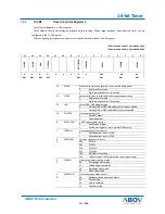
16-bit Timer
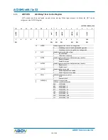
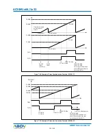
The update timing of Data0 and Data1 buffer in dynamic operation, is different in each operating mode and is depends
on the Tn.CR1.UAO bit.
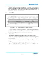
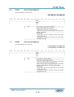
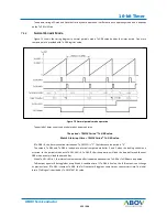
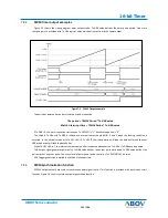
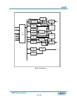
Normal Periodic Mode
7.4.2
Figure 7.3 shows the timing diagram in normal periodic mode. Tn.GRB value decides the timer period. One more
compare point is provided with Tn.GRA register value.
Figure 7.3 Normal periodic mode operation
The period of timer count can be calculated as below equation.
The period = TMCLK Period * Tn.GRB value.
Match A interrupt time = TMCLK Period * Tn.GRA value.
If Tn.GRB = 0, the timer cannot be started even Tn.CR2.TEN is “1”. That’s because the period is “0”.
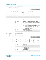
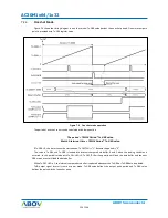
The value in Tn.GRA and Tn.GRB is loaded into internal compare data buffer 0 and 1 when the loading condition is
occurred. In this periodic mode with Tn.CR1.UAO =0, Tn.CR2.TCLR write operation will load the data buffer and the next
GRB match event will load the data buffer.
When Tn.CR1.UAO is 1, the internal compare data buffer is updated whenever the Tn.GRA or Tn.GRB data is updated.
TnIO output signal will be toggled at every Match A condition time. If Tn.GRA is 0 value, the TnIO output is not change
its previous level. If Tn.GRA is same as Tn.GRB, the TnIO output will toggle at same time as counter start time. The initial
level of TnIO signal is decided by Tn.CR1.STARTLVL value.
Summary of Contents for AC30M1x32
Page 3: ...3 246 ABOV Semiconductor INTRODUCTION SECTION 1 INTRODUCTION ...
Page 4: ...4 246 4 246 AC30M1x64 1x32 ABOV Semiconductor OVERVIEW CHAPTER 1 ...
Page 18: ...18 246 18 246 ABOV Semiconductor AC30M1x64 1x32 CPU CHAPTER 2 ...
Page 22: ...22 246 22 246 ABOV Semiconductor AC30M1x64 1x32 Boot Mode CHAPTER 3 ...
Page 26: ...26 246 26 246 ABOV Semiconductor AC30M1x64 1x32 SECTION 2 PERIPHERALS ...
Page 27: ...27 246 ABOV Semiconductor System Control Unit SCU SYSTEM CONTROL UNIT SCU CHAPTER 1 ...
Page 69: ...69 246 ABOV Semiconductor Port Control Unit PCU PORT CONTROL UNIT PCU CHAPTER 2 ...
Page 85: ...85 246 ABOV Semiconductor General Purpose I O GPIO GENERAL PURPOSE I O GPIO CHAPTER 3 ...
Page 92: ...92 246 92 246 AC30M1x64 1x32 ABOV Semiconductor FLASH MEMORY CONTROLLER CHAPTER 4 ...
Page 105: ...105 246 ABOV Semiconductor Internal SRAM INTERNAL SRAM CHAPTER 5 ...
Page 107: ...107 246 ABOV Semiconductor Watch Dog Timer WATCH DOG TIMER WDT CHAPTER 6 ...
Page 113: ...113 246 ABOV Semiconductor 16 bit Timer 16 BIT TIMER CHAPTER 7 ...
Page 129: ...129 246 ABOV Semiconductor FRT FREE RUN TIMER FRT CHAPTER 8 ...
Page 134: ...134 246 134 246 ABOV Semiconductor AC30M1x64 1x32 FUNCTION DESCRIPTION 8 3 ...
Page 135: ...135 246 UART ABOV Semiconductor UNIVERSAL ASYNCHRONOUS CHAPTER 9 RECEIVER TRANSMITTER UART ...
Page 151: ...151 246 ABOV Semiconductor UART Figure 9 6 Transmit interrupt timing diagram ...
Page 152: ...152 246 152 246 ABOV Semiconductor AC30M1x64 1x32 SERIAL PERIPHERAL INTERFACE SPI CHAPTER 10 ...
Page 164: ...164 246 164 246 ABOV Semiconductor AC30M1x64 1x32 I2 C Interface CHAPTER 11 ...
Page 185: ...185 246 ABOV Semiconductor Motor PWM MOTOR PULSE WIDTH MODULATOR CHAPTER 12 MPWM ...
Page 215: ...215 246 ABOV Semiconductor Divider DIVIDER DIV64 CHAPTER 13 ...
Page 221: ...221 246 ABOV Semiconductor 12 BIT A D Converter 12BIT A D CONVERTER CHAPTER 14 ...
Page 235: ...235 246 ABOV Semiconductor CHARACTERISTIC SECTION 3 CHARACTERISTIC ...
Page 236: ...236 246 236 246 ABOV Semiconductor AC30M1x64 1x32 Electrical Characteristic CHAPTER 1 ...
Page 243: ...243 246 ABOV Semiconductor Package Package CHAPTER 2 ...