Power Automation and Protection Division
I.L. 40-201.9
REL 352 Version 1.00
E-1
E
A
P
P
E
N
D
I
X
MICROPROCESSOR MODULE
Schematic - - - - - - - - - - - - - - - - - - - - - - - - - - - - - - - - 1612C18
Component Location Diagram - - - - - - - - - - - - - - - - - - 1611C22
1
ARCHITECTURE
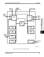
The block diagram of this module is shown in Figure E-1. Each block in the figure has a location designator with
the following convention (for example, 2/U16):
NOTE:
For clarity, the supporting components, e.g., transparent latches, address decode PALs,
buffers, drivers, etc., are not shown on the block diagram.
Each Processor (P1 and P2) contains the following elements:
• Microprocessor – 16 bit microcontroller (Intel 80C196), operating at a clock fre-
quency of 12 MHz
• EPROM
– an ultraviolet, erasable read-only memory for program storage.
• RAM
– a read-write, static, volatile memory for temporary data storage.
• EEPROM
– electrically erasable, read-write memory for settings and fault-
data storage.
• I/O Interface
– for power system control (relay outputs and contact inputs); al-
so, interfaces with a communication Modem and analog/digital
subsystem.
Additionally, Processor P1 accesses real-time clock (U16), which contains a battery for non-volatile operation
in the absence of power.
Both processor systems are interconnected via the dual port RAM 2k x 16 (U32). This device has 2 separate
ports; each port permits independent asynchronous access for reads and writes to any memory location. The
chip arbitration logic resolves any contentions for memory access.
2
MEMORY MAPS
Memory maps for Processors P1 and P2 are shown in Figures E-2 and E-3, respectively.
The 80C196 microcontroller supports 64K bytes of address space directly. This is adequate for Processor 2, but
Processor 1 requires more than 64K of address space because of the large RAM requirement for oscillographic
data collection. The INST output of the microcontroller is used to decode 64K of program memory and 64K of
data memory separately.
3
TASK ASSIGNMENT
The processors perform the following major tasks:
Processor 1
• Analog input sampling and Fourier computations
• Operator interface
• INCOM communications
• Non-volatile data storage with 2-out-of-3 memory sampling (voting)
Schematic Page #
IC Number
2
U16


