82 CP9*, CR9*, CT9* Celeron M/Pentium M
Publication No. HRMCP9 Rev. B
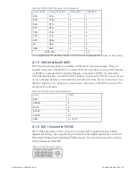
Table A-7 DVI Connector Digital Pin Assignments
Pin
Signal name
Pin
Signal name
1
TX2- (TMDS Data2–)
13
NC
2
TX2+ (TMDS Data2+)
14
FUSE_VCC
a
3
GND
15
GND
4
NC
16
NC
5
NC
17
TX0- (TMDS Data0–)
6
DDC Clock
18
TX0+ (TMDS Data0+)
7
DDC Data
19
GND
8
VSYNC
20
NC
9
TX1- (TMDS Data1–)
21
NC
10
TX1+ (TMDS Data1+)
22
GND
11
GND
23
TXC+ (TMDS Clock+)
12
NC
24
TXC- (TMDS Clock–)
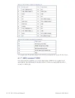
Table A-8 DVI Connector Analog Pin Assignments
Pin
Signal name
C1
RED Analog Red Video
C2
GREEN Analog Green Video
C3
BLUE Analog Blue Video
C4
HSYNC Analog Horizontal Sync
C5
GND
a
+5 V supplied by the CR9 and fused with max 2 A at CTM12 for normal operation don’t exceed 100 mA at this pin.
A.1.7 USB Connector P2005
Four channels are available on a 10-pin male header. USBVCC is supplied and
controlled by the CR9 board. It is fused with 2 A, but for normal operation don’t
exceed 1 A at this pin.

