Z8018x
Family MPU User Manual
20
UM005004-0918
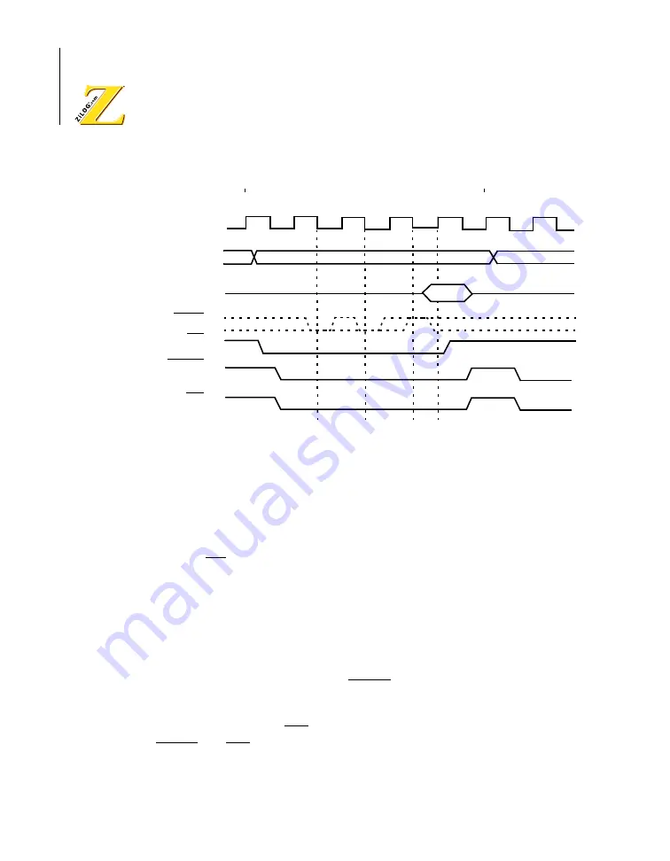
Figure 10. Op Code Fetch (with Wait State) Timing Diagram
Operand and Data Read/Write Timing
The instruction operand and data read/write timing differs from Op Code
fetch timing in two ways:
•
The M1 output is held inactive
•
The read cycle timing is relaxed by one-half clock cycle because data
is latched at the falling edge of T3
Instruction operands include immediate data, displacement, and extended
addresses, and contain the same timing as memory data reads.
During memory write cycles the MREQ signal goes active in the second
half of T1. At the end of T1, the data bus is driven with the write data.
At the start of T2, the WR signal is asserted Low enabling the memory.
MREQ and WR go inactive in the second half of T3 followed by
disabling of the write data on the data bus.
T1
T2
T2
TW
TW
T3
T1
Phi
A0
–
A19
D0
–
D7
M1
MREQ
RD
WAIT
Op Code
Содержание Z8018 Series
Страница 1: ...www zilog com Z8018x Family MPU User Manual UM005004 0918...
Страница 206: ...Z8018x Family MPU User Manual 192 UM005004 0918...
Страница 220: ...Z8018x Family MPU User Manual 206 UM005004 0918...
Страница 250: ...Z8018x Family MPU User Manual 236 UM005004 0918...
Страница 260: ...Z8018x Family MPU User Manual 246 UM005004 0918...
Страница 300: ...Z8018x Family MPU User Manual 286 UM005004 0918...
Страница 306: ...Z8018x Family MPU User Manual 292 UM005004 0918...


