16
Circuit Description
The resulting DC squelch control voltage is passed
to pin 19 of the microprocessor Q1048. If no carrier
is received, this signal causes pin 32 of Q1048 to go
low and pin 89 to go high. Pin 32 signals Q1008
(
CPH6102
), Q1064 and Q1065 (both
UMC5N
) to dis-
able the supply voltage to the audio amplifier Q1017
and Q1063, while pin 89 makes Q1014 (
UMG2N
) hold
the green (Busy) half of the LED off.
Thus, the microprocessor blocks output from the
audio amplifier, and silences the receiver while no
signal is being received, and during transmission.
When a carrier appears at the discriminator, noise
is removed from the output, causing pin 19 of Q1048
to go low and the microprocessor to activate the Busy
LED via Q1048.
The microprocessor then checks for DTMF or CTCSS
or CDCSS code squelch information, if enabled, re-
spectively. If not transmitting and CTCSS or CDCSS
is not activated, or if the received tone or code
matches that programmed, the microprocessor stops
scanning, if active, and allows audio to pass through
the audio amplifier (Q1017 or Q1063) to the loud-
speaker by enabling the supply voltage to it via
Q1008, Q1064, and Q1065.
Transmit Signal Path
Microphone amplifier
Speech input from the microphone is amplified in
Q1022 (
NJM2902V
), then filtered and sent to Q1025
(
M62364FP
), then on to the Dummy Unit (or an
Optional Unit). The audio which is returned from
the Dummy Unit passes through Q1028 (
AK2345
)
to be pre-emphasized.
The processed audio is then mixed with a CTCSS
tone generated by Q1028 (
AK2345
) and delivered
to D1035 (
HVU350
) for frequency modulating the
PLL carrier up to ±5kHz from the unmodulated car-
rier at the transmitting frequency.
If an external microphone is used, PTT switching is
controlled by Q1007 (
UMZ2N
), which signals the
microprocessor when the impedance at the micro-
phone jack drops.
If a CDCSS code is enabled for transmission, the code
is generated by microprocessor Q1048 and delivered
to D1055 (
HVC350
) for CDCSS modulating.
If DTMF is enabled for transmission, the tone is gen-
erated by the microprocessor Q1048 and applied to
the splatter filter section in place of speech audio.
Also, the tone is amplified for monitoring in the
loudspeaker.
Noise canceling microphone circuit
The two signals from internal microphone (main and
sub) are injected to the positive input (sub) and to
the negative input (main) of Q1022 (
NJM2902V
). If
the same signal is injected to both the main and sub
ports, the main signal is canceled at the output (pin
7 of Q1022). In other words, noise from nearby
sources not directly connected to the transceiver en-
ters the main and sub input at the same signal level
and is therefore canceled out.
When a signal is only injected to the “main” port
and there is no signal at sub, the main signal is al-
lowed to flow, as is, from Q1022.
Driver and Final Amplifiers
The modulated signal from the VCO Q1039
(
2SC4227
) is buffered by Q1034 (
2SC5226-4/5
) and
amplified by Q1030 (
2SC5226-4/5
) and Q1060
(
2SC3356-R25
). The low-level transmit signal is then
applied to the Power Module Q1019 (
M68732HA-
22
) for final amplification up to 5 watts output power.
The transmit signal then passes through the antenna
switch D1020 (
HVU131
) and is low-pass filtered to
suppress away harmonic spurious radiation before
delivery to the antenna.
Automatic Transmit Power Control
RF power output from the final amplifier is sampled
by C1016 and C1018, and is rectified by D1019
(
RB715F
). The resulting DC voltage is fed back
through Q1018 (
NJM2902V
) to the Power Module,
providing control of the power output.
The microprocessor selects either “High” or one of
three “Low” power levels.
Transmit Inhibit
When the transmit PLL is unlocked, pin 18 of PLL
chip Q1054 goes to a logic low. The resulting DC
unlock control voltage is passed to pin 20 of the mi-
croprocessor Q1048. While the transmit PLL is un-
locked, pin 85 of Q1048 remains low, which then
turns off the Automatic Power Controller Q1010
Содержание VX-800
Страница 10: ...10 Set Menu Mode Functions Note ...
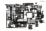
Страница 13: ...13 Block Diagram ...
Страница 14: ...14 Note Block Diagram ...
Страница 24: ...24 Note ...
Страница 26: ...26 Main Unit Lot 1 3 Note ...
Страница 29: ...29 Main Unit Lot 4 50 Circuit Diagram ...
Страница 30: ...30 Main Unit Lot 4 50 Note ...
Страница 33: ...33 Main Unit Lot 51 Circuit Diagram ...
Страница 34: ...34 Main Unit Lot 51 Note ...

