


Version 160624
Page 17
minimize ground loop noise. The cable should be twisted pair with individual shields, even when driven by an
unbalanced source.
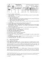
6.5
Analog Audio Output Connections
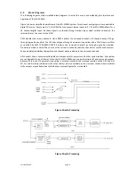
The JSD-100MA provides sixteen main channel outputs. All outputs are balanced and may drive balanced or
unbalanced loads. When driving unbalanced loads, run two conductor shielded cable and connect the “ – ”
terminal of the JSD-100MA output to the low side of the unbalanced load at the load instead of at the JSD-
100MA to minimize ground loop noise.
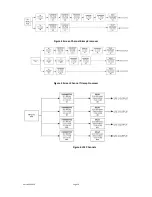
6.5.1 Main Audio Outputs
The main audio outputs are on a module that can be replaced from the rear. To allow for proper bypass
operation, a passive crossover is included. For full band operation, set all four DIP switches to OFF and set the
MID and HIGH trim pots to full counter-clockwise. Adjust the LOW trim pot for the desired full range bypass
audio level. Remember that the front panel fader also affects output level when in bypass. For bypass
operation with crossovers, see Section 7.5.1. The connections for these output modules are detailed in
Appendix A.
6.5.2 HI/VI-N Outputs
The JSD-100MA has balanced HI and VI-N outputs that can drive balanced or unbalanced loads. As with other
outputs, the use of twisted pair shielded cable is suggested whether the load is balanced or unbalanced. When
driving an unbalanced load, connect the “–” output of the JSD-100MA to low side of the unbalanced input at
the destination end of the cable to minimize ground loop noise. The source of audio to drive the HI and VI-N
outputs is configurable on a per-format basis. The USL supplied ferrite block should be clipped on to the
cables adjacent to the connectors to comply with FCC and CE emission requirements. See Appendix A for pin
out information.
6.6
Automation Interface
The JSD-100MA includes the traditional parallel automation interface plus RS-232 and Ethernet. See appendix
B for a list of the automation commands.
6.6.1 Parallel Interface
Pins 1 through 10 of the DB25F automation connector are “control” pins that accept contact closure or open
collector pulses to ground to select formats. On a format change, the corresponding pin is also pulsed low
allowing this interface to drive other equipment. Pulsing pin 11 low toggles the mute state. Pins 14 through
24 are “status” pins. One of the pins 14 through 23 is pulled low continuously by the JSD-100MA to indicate
the selected format. These pins could drive LEDs with a 470 ohm series resistor to provide a remote format
indication. The JSD-100MA pulls pin 24 low when the system is muted. Pins 1 through 11 are internally pulled
up to +8.4V. They each source 400uA when grounded. A pin needs to be pulled below 2.6V for 10ms or more
for the JSD-100MA to recognize it as low. On a format change, the JSD-100MA pulls the appropriate pin low for
500ms. +5V at 100mA is available on pin 13 to drive external LEDs or relays. The individual control and status
outputs can sink up to 150mA with an open circuit voltage of +12VDC for inductive loads like relays or +24V for
non-inductive loads (indicator lamps, etc.). Pin 12 is the “automation return.” Use this as the low side of
switches and indicators instead of using chassis ground. It is ground through a 10 ohm resistor to limit ground
loop current. The USL supplied ferrite block should be clipped on to the cables adjacent to the connectors to
comply with FCC and CE emission requirements. See Appendix A for pin out information.
6.6.2 RS-232 Interface
The RS-232 interface appears on a DE9F connector on the rear panel. The connector is wired as a DCE device.
A command interpreter accepts ASCII commands over the RS-232 and Ethernet interfaces. The RS-232 port
operates at 38.4kbps, 8N1 (8 data bits, no parity, 1 stop bit), hardware handshake. In most situations, no
handshake is required, and the RTS and CTS pins can be left open. The USL supplied ferrite block should be
clipped on to the cables adjacent to the connectors to comply with FCC and CE emission requirements. See
Appendix A for the connector pin out.


