


NINA-W1 series - System integration manual
UBX-17005730 - R15
System description
Page 7 of 54
C1 - Public
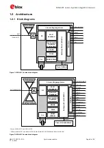
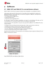
* Only on NINA-W152 and NINA-W152
** Only on NINA-W156. Support in u-connectXpress – pending implementation
Figure 3: NINA-W15 series block diagram
1.3
CPU
NINA-W1 series modules use a dual-core system that includes two Harvard Architecture Xtensa LX6
CPUs with maximum 240 MHz internal clock frequency. The internal memory of NINA-W1 supports:
•
448 kB ROM for booting and core functions
•
520 kB SRAM for data and instruction
•
16 or 32 Mbit FLASH memory for code storage, including hardware encryption to protect programs
and data.
•
1 kbit EFUSE (non- erasable memory) for MAC addresses, module configuration, flash-encryption,
and Chip-ID.
Open CPU variants (NINA-W10) also support external FLASH and SRAM memory through a Quad SPI
interface.
1.4
Operating modes
1.4.1
Power modes
NINA-W1 series modules are power efficient devices capable of operating in different power saving
modes and configurations. Different sections of the modules can be powered off when they are not
needed, and complex wake up events can be generated from different external and internal inputs.
For details on the available power modes, see the data sheet for the corresponding module [2][3][4].
Flash (16 Mbit)
Linear voltage regulators
RF
ROM
Wi-Fi
baseband
IO
b
u
ff
ers
2
xX
ten
sa
3
2
-bi
t L
X
6
MC
U
SRAM (4Mbit)
Cryptographic
hardware
accelerations
PIFA antenna
(NINA-W152)
PLL
Quad SPI
VCC_IO
VCC (3.0-3.6 V)
40 MHz
Reset
UART
RMII
EFUSE
GPIO
BPF*
(NINA-W151)
ANT
Wi-Fi
baseband
(NINA-W156)
PCB trace antenna
SPI
LPO**


