NINA-W1 series - System integration manual
UBX-17005730 - R15
Design-in
Page 38 of 54
C1 - Public
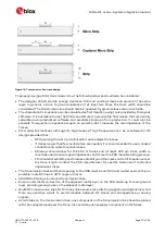
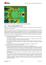
Figure 23: Size of the GND cut out for the NINA-W1x6 module’s PCB trace antenna
3.4
Data communication interfaces
3.4.1
Asynchronous serial interface (UART) design
The layout of the UART bus should be done so that noise injection and cross talk are avoided. It is
recommended to use the hardware flow control with RTS/CTS to prevent temporary UART buffer
overrun.
The flow control signals
RTS/CTS
are active low. Consequently, 0 (ON state =low level) allows the
UART to transmit.
•
CTS
is an input to the NINA-W1 module. If the host sets this input to 0 (ON state = low level) the
module can transmit.
•
RTS
is an output off the NINA-W1 module. The module sets the output to 0 (ON state = low level)
when it is ready to receive transmission.
3.4.2
Ethernet (RMII+SMI)
It is recommended to route all signals in the RMII bus with the same length and have appropriate
grounding in the surrounding layers; total bus length should also be minimized. The layout of the RMII
bus should be done so that crosstalk with other parts of the circuit is minimized providing adequate
isolation between the signals, the clock and the surrounding busses/traces.
Termination resistors are recommended for the RX and TX lines on the RMII bus.
A pull-up resistor is required for
RMII_MDIO
and
RMII_CRSDV
.
General high-speed layout guidelines
are applicable for the RMII and SMI bus.
3.5
General high-speed layout guidelines
These general design guidelines are considered as best practices and are valid for any bus present in
the NINA-W1 series modules. The designer should prioritize the layout of higher speed busses. Low
frequency signals are generally not critical for layout.
☞
One exception is represented by High Impedance traces (such as signals driven by weak pull
resistors) that may be affected by crosstalk. For those traces, supplementary 4W isolation from
other busses is recommended.


