


L M K 0 4 9 0 6 E V A L U A T I O N B O A R D O P E R A T I N G I N S T R U C T I O N S
SNAU126
37
Appendix B: Typical Phase Noise Performance Plots
PLL1
The LMK04906B‟s dual PLL architecture achieves ultra low jitter and phase noise by allowing
the external VCXO or Crystal‟s phase noise to dominate the final output phase noise at low
offset frequencies and the internal VCO‟s phase noise to dominate the final output phase noise at
high offset frequencies. This results in the best overall noise and jitter performance.
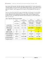
Table 11 lists the test conditions used for output clock phase noise measurements with the
Crystek 122.88 MHz VCXO.
Table 11: LMK04906B Test Conditions
Parameter
Value
PLL1 Reference clock input
CLKin0 single-ended input, CLKin0* AC-coupled to GND
PLL1 Reference Clock frequency 122.88 MHz
PLL1 Phase detector frequency
122.88 MHz
PLL1 Charge Pump Gain
100 uA
VCXO frequency
122.88 MHz
PLL2 phase detector frequency
122.88 MHz
PLL2 Charge Pump Gain
3200 uA
PLL2 REF2X mode
Disabled
122.88 MHz VCXO Phase Noise
The phase noise of the reference is masked by the phase noise of this VCXO by using a narrow
loop bandwidth for PLL1 while retaining the frequency accuracy of the reference clock input.
This VCXO sets the reference noise to PLL2. Figure 15 shows the open loop typical phase noise
performance of the CVHD-950-122.88 Crystek VCXO.


