


L M K 0 4 9 0 6 E V A L U A T I O N B O A R D O P E R A T I N G I N S T R U C T I O N S
SNAU126
11
PLL Loop Filters and Loop Parameters
In jitter cleaning applications that use a cascaded or dual PLL architecture, the first PLL‟s
purpose is to substitute the phase noise of a low-noise oscillator (VCXO or crystal resonator) for
the phase noise of a “dirty” reference clock. The first PLL is typically configured with a narrow
loop bandwidth in order to minimize the impact of the reference clock phase noise. The reference
clock consequently serves only as a frequency reference rather than a phase reference.
The loop filters on the LMK04906 evaluation board are setup using the approach above. The
loop filter for PLL1 has been configured for a narrow loop bandwidth (< 100 Hz), while the loop
filter of PLL2 has been configured for a wide loop bandwidth (> 100 kHz). The specific loop
bandwidth values depend on the phase noise performance of the oscillator mounted on the board.
The following tables contain the parameters for PLL1 and PLL2 for each oscillator option.
TI‟s Clock Design Tool can be used to optimize PLL phase noise/jitter for given specifications.
See:
http://www.ti.com/tool/codeloader
.
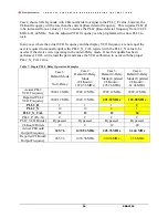
PLL 1 Loop Filter
Table 4: PLL1 Loop Filter Parameters for Crystek 122.88 MHz VCXO
122.88 MHz VCXO PLL
Phase Margin
49˚
Kφ (Charge Pump)
100 uA
Loop Bandwidth
12 Hz
Phase Detector Freq
1.024 MHz
VCO Gain
2.5 kHz/Volt
Reference Clock
Frequency
122.88 MHz
Output Frequency
122.88 MHz (To PLL 2)
Loop Filter
Components
C1_A1 = 100 nF
C2_A1 = 680 nF
R2_A1 = 39 kΩ
Note:
PLL Loop Bandwidth is a function of K , Kvco, N as well as loop components. Changing
K and N will change the loop bandwidth.


