


L M K 0 4 9 0 6 E V A L U A T I O N B O A R D O P E R A T I N G I N S T R U C T I O N S
SNAU126
23
Single Loop 0-Delay Mode Examples
In Single Loop 0-Delay Mode, MODE = 8, the feedback from the VCO of PLL2 to the
PLL2_P/PLL2 N divider is broken and a fed back clock output will drive the PLL2 N divider
directly. This permits phase alignment between the clock output and the OSCin input (0-Delay).
As such, the PLL2_N, PLL2_R, and PLL2_N_CAL divide values may need to be adjusted to
permit the LMK04906 to lock.
Programming Steps
1.
Program the Single Loop 0-Delay mode.
2.
Enable the feedback mux. EN_FEEDBACK_MUX = 1.
3.
Select clock output for feedback with the feedback mux. FEEDBACK_MUX = User
value.
4.
Program the VCO frequency of PLL2 tab to: The actual VCO frequency * PLL2_P
(which is PLL2 PreN) / CLKout Divider.
Entered CodeLoader 4 VCO Frequency = Actual VCO Frequency * PLL2_P /
CLKout Divider.
5.
Updated the PLL2_N_CAL register on the Bits/Pins tab to the N value when in non-0-
Delay mode.
6.
Press Ctrl-L to cause all registers to be programmed.
The reason is to cause the programming of register R30 to start the VCO
calibration routine now that the proper PLL2_N_CAL value is programmed.
PLL2_N_CAL value is automatically updated when a new VCO frequency is
entered and the PLL2_N value is calculated. In this case the VCO frequency
entered is wrong and the PLL2_N_CAL value will be incorrect.
If for any reason the CLKout frequency is less than the phase detector frequency, the PLL2 R
divider must be increased so that the phase detector is at the same or lower value than the
CLKout frequency.
Details
The 0-Delay mode for Single Loop mode is more complicated to program than for Dual Loop
mode in part because of the PLL2_N_CAL register. When performing the VCO calibration the
device uses PLL2_N_CAL for in non-0-Delay mode. Once the VCO is calibrated the device
enters 0-Delay mode. For more information on the PLL programming equations, refer to PLL
PROGRAMMING in the applications section of the datasheet.
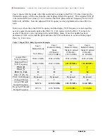
In Table 7 case 1 illustrates the register programming when note using 0-Delay.
Case 2 shows 0-Delay with a clock out divider of 2. Since PLL2_P = 2, this substitution of
which circuit is performing the divide by two results in no impact o the software. All the values
display correctly.
Case 3 shows 0-Delay mode with a CLKout divider not equal to the PLL2_P value. So the
proper frequency to program in the VCO to lock the VCO to 2949.12 MHz will be 491.52 MHz.
This is calculated by Actual VCO Frequency * PLL2_P / CLKoutX_Y_DIV.


