3.4.2
JTAG Connector
Hardware Configuration
www.ti.com
sample boundaries in the serial data stream. The frame clock line is unused in the parallel LVDS DDR
format. In addition, 14 extra LVDS pairs are defined in the connector and routed to the TSW1200EVM
FPGA for future expansion for larger parallel bus widths needed for faster data converters. The data
direction for the LVDS data pairs is always defined as the ADC EVM driving the signal through the
connector to the TSW1200EVM FPGA, with integrated 100-
Ω
termination in the FPGA.
For one-channel parallel DDR bit-wise data formats, eight of the LVDS data pairs are used to support up
to 16-bit-resolution ADCs at up to 250-MHz sampling rates. For one-channel parallel DDR sample-wise
data formats, 14 of the LVDS data pairs are used to support up to 14-bit-resolution ADCs at up to
500-MHz sampling rates. For two-channel parallel DDR bit-wise data formats, 14 of the LVDS data pairs
are used to support two channels of 14-bit resolution at up to 250-MHz sampling rate.
For serial data formats, eight of the LVDS data pairs support up to eight channels of one-wire serial ADCs
at up to 65-MHz sampling rate or four channels of two-wire serial ADCs at up to 125-MHz sampling rates.
All other LVDS pairs are ignored for this release.
Five extra CMOS single-ended signals are defined in the Samtec connector that are sourced from the
FPGA through the connector to the ADC EVM. These signals are optionally defined to allow the FPGA
(under control of the TSW1200 user interface software) control the SPI serial programming of the ADC for
those ADC EVMs that support this feature. For those ADC EVMs that support this feature, the SPI signals
SEN (SPI Enable), SCLK (SPI Clk), and SDATA (SPI Data) are sourced by the TSW1200EVM FPGA to
allow the TSW1200 user Interface to configure the operational mode of the ADC under evaluation. There
SPI signals are by default not connected on the ADC EVM until a 0-
Ω
resistor is installed on the EVM to
enable control of the SPI port from the TSW1200 user Interface software. Two additional signals, SPI
Reset and SPI Power Down, are defined for possible future use.
The Samtec connectors snap together with no screws or other mechanism to hold the TSW1200EVM and
the ADC EVM together. The TSW1200EVM comes with standoff posts for setting the TSW1200EVM flat
on a bench or table. The ADC EVM has shorter standoff posts so that the TSW1200EVM and ADC EVM
will lay flat on a bench or table and stay snapped together during use.
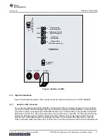
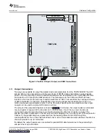
The TSW1200EVM includes an industry-standard JTAG connector that loops the JTAG ports of the FPGA
and the FPGA EEPROM. Jumpers on the TSW1200EVM allow for either the FPGA or the FPGA
EEPROM to be removed from the JTAG chain. The most frequent use for the JTAG connector is to
program the TSW1200EVM FPGA. An FPGA programming pod can be purchased inexpensively from
Xilinx™ to program the FPGA or the FPGA EEPROM.
The FPGA programming pod can be used to load a programming bit file directly into the FPGA for debug
and development. However, once the FPGA is power-cycled or programmed by the PROGRAM
pushbutton, this loaded FPGA bit file will be lost and the FPGA will revert to the bit file that is stored in the
FPGA EEPROM. The FPGA programming pod also can be used to store a new FPGA programming bit
file in the FPGA EEPROM so that the TSW1200 can be upgraded as new revisions of FPGA firmware
become available.
The part number of the Xilinx Platform Cable USB programming pod that can be used to program or
upgrade the TSW1200EVM is
DLC9G
. The programming pod operates from a USB port of a PC and
connects directly with the TSW1200 JTAG connector through a ribbon cable supplied with the
programming pod.
10
TSW1200EVM: High-Speed LVDS Deserializer and Analysis System
SLAU212A – April 2007 – Revised August 2008


