


19
18
17
16
15
14
13
12
11
10
9
8
7
6
5
4
3
2
1
0
19
18
17
16
15
14
13
12
11
10
9
8
7
6
5
4
3
2
1
0
1
P
5
/8
V
T
D
A
0
..
1
9
T
D
A
0
..
1
9
R
D
A
0
..
1
9
G
N
D
G
N
D
JMP145
JMP38
JMP37
G
N
D
G
N
D
T
X
C
L
K
A
R
X
C
L
K
A
PARALLEL SIGNAL
BIT NUMBER
PARALLEL SIGNAL
BIT NUMBER
PIN TYPE OF ROW
PIN NAMES
www.ti.com
Parallel Signals
11
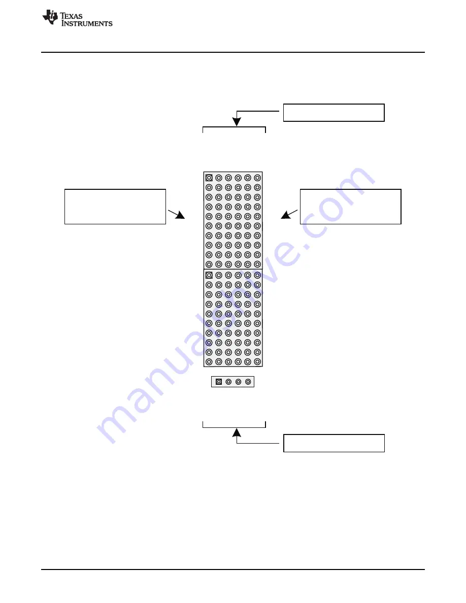
Parallel Signals
The parallel signals on the TLK6002EVM have been routed to a 0.1-in. header block that is configured like
Figure 13
. All RD pins on header blocks RDA/B[7:0], RDA/B[15:8], as well as all TDA/B pins on header
blocks TDA/B[7:0], TDA/B[15:8], have matched trace lengths to themselves ±0.5 mil.
Figure 13. Parallel Signal Header Block Diagram
Parallel Loopback, shown in
Figure 14
, can be easily implemented by placing jumpers on the RDx/TDx
pins of the header. For example, placing a jumper on pins 4 and 5 of JMP37 loops back TDA19 to
RDA19.
The Transmit Data Clocks and Receive Data Clocks are located in header blocks JMP145 and JMP146
with the clock pins next to each other. These signals are the parallel side input and output clocks per
channel. During Parallel Loopback, the clocks can be shorted together as shown in
Figure 14
.
21
SLLU132 – October 2010
TLK6002 Dual-Channel, 0.47-Gbps to 6.25-Gbps, Multi-Rate Transceiver
Evaluation Module
Submit Documentation Feedback
Copyright © 2010, Texas Instruments Incorporated