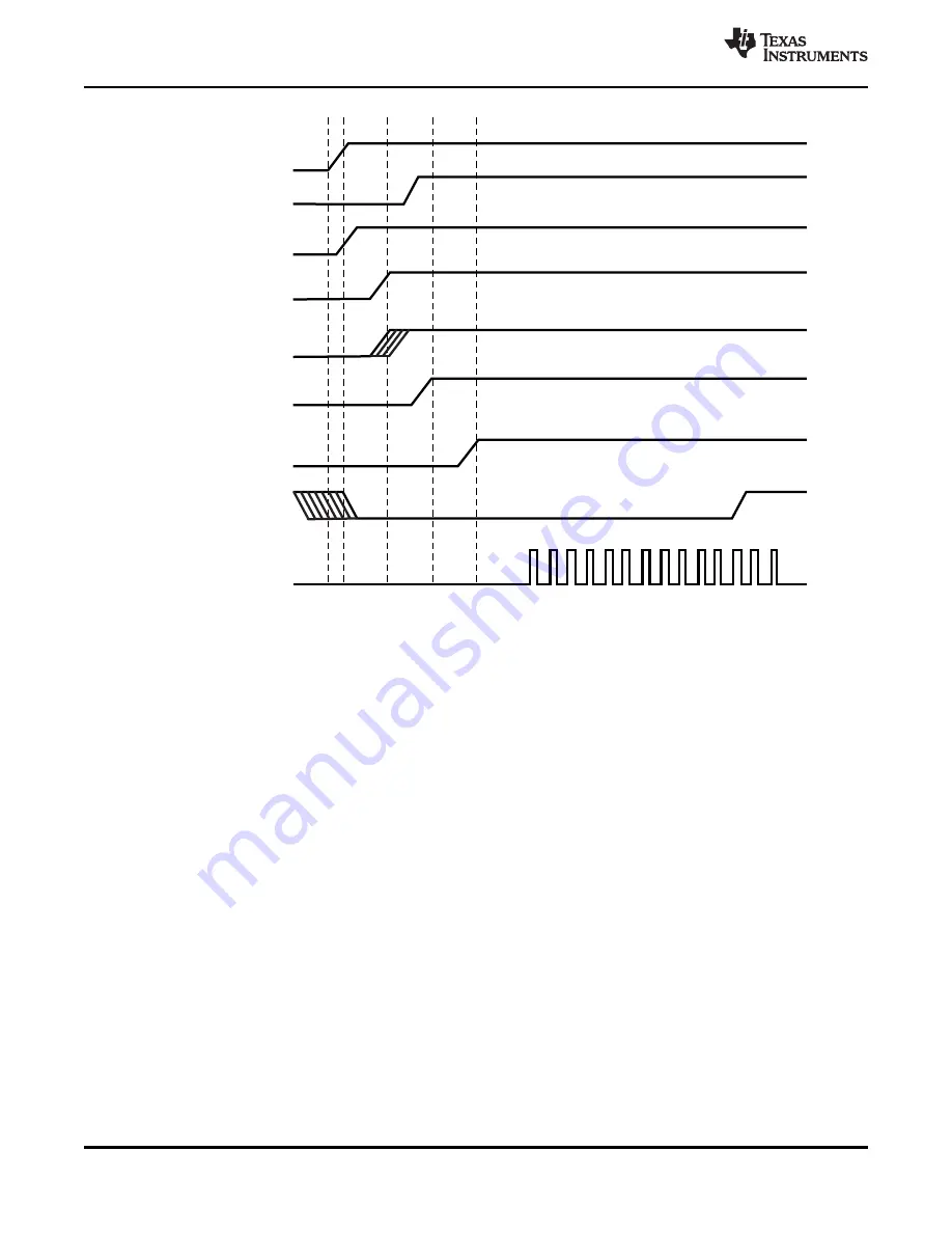
VDDS_RTC
RTC_PWRONRSTn
PMIC_POWER_EN
VDDS_DDR
All 1.8-V Supplies
IO 3.3-V Supplies
VDD_CORE, VDD_MPU
PWRONRSTn
CLK_M_OSC
1.8V
1.8V
1.8V
1.8V
1.8V/1.5V/1.35V
3.3V
1.1V
AM3359, AM3358, AM3357, AM3356, AM3354, AM3352
SPRS717H – OCTOBER 2011 – REVISED MAY 2015
A.
RTC_PWRONRSTn should be asserted for at least 1 ms to provide enough time for the internal RTC LDO output to
reach a valid level before RTC reset is released.
B.
When using the ZCZ package option, VDD_MPU and VDD_CORE power inputs may be powered from the same
source if the application only uses operating performance points (OPPs) that define a common power supply voltage
for VDD_MPU and VDD_CORE. The ZCE package option has the VDD_MPU domain merged with the VDD_CORE
domain.
C.
If a USB port is not used, the respective VDDA1P8V_USB terminal may be connected to any 1.8-V power supply and
the respective VDDA3P3V_USB terminal may be connected to any 3.3-V power supply. If the system does not have a
3.3-V power supply, the VDDA3P3V_USB terminal may be connected to ground.
D.
If the system uses mDDR or DDR2 memory devices, VDDS_DDR can be ramped simultaneously with the other 1.8-V
IO power supplies.
E.
VDDS_RTC can be ramped independent of other power supplies if PMIC_POWER_EN functionality is not required. If
VDDS_RTC is ramped after VDD_CORE, there might be a small amount of additional leakage current on
VDD_CORE. The power sequence shown provides the lowest leakage option.
F.
To configure VDDSHVx [1-6] as 1.8 V, power up the respective VDDSHVx [1-6] to 1.8 V following the recommended
sequence. To configure VDDSHVx [1-6] as 3.3 V, power up the respective VDDSHVx [1-6] to 3.3 V following the
recommended sequence.
Figure 6-2. Preferred Power-Supply Sequencing With Dual-Voltage IOs Configured as 3.3 V
100
Power and Clocking
Copyright © 2011–2015, Texas Instruments Incorporated
Product Folder Links:


