MSP430FG47x
MIXED SIGNAL MICROCONTROLLER
SLAS580D -- OCTOBER 2008 -- REVISED MARCH 2011
9
POST OFFICE BOX 655303
DALLAS, TEXAS 75265
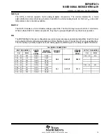
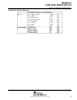
Terminal Functions (continued)
TERMINAL
NO.
I/O
DESCRIPTION
NAME
80
PIN
113
PIN
I/O
DESCRIPTION
S17
24
L4
O
LCD segment output 17
S18
25
M4
O
LCD segment output 18
S19
26
J4
O
LCD segment output 19
S22
29
L6
O
LCD segment output 22
S23
30
M6
O
LCD segment output 23
S24
31
L7
O
LCD segment output 24
S25
32
M7
O
LCD segment output 25
GND
7
E2
Ground. It is used to shield the oscillator. See Note 1.
XIN
8
E1
I
Input port for crystal oscillator XT1. Standard or watch crystals can be connected.
XOUT
9
F1
O
Output port for crystal oscillator XT1. Standard or watch crystals can be connected.
GND
10
F2
Ground. It is used to shield the oscillator. See Note NO TAG.
V
REF
60
A12
O
Input for an external reference voltage/internal reference voltage output
RST/NMI
74
B5
I
Reset input, nonmaskable interrupt input port, or bootstrap loader start (in flash devices).
TCK
73
A5
I
Test clock (JTAG). TCK is the clock input port for device programming test and bootstrap loader
start.
TDI/TCLK
71
A6
I
Test data input or test clock input. The device protection fuse is connected to TDI/TCLK.
TDO/TDI
70
B7
I/O
Test data output port. TDO/TDI data output or programming data input terminal.
TMS
72
B6
I
Test mode select. TMS is used as an input port for device programming and test.
XT2OUT
68
A8
O
Output terminal of crystal oscillator XT2
XT2IN
69
A7
I
Input port for crystal oscillator XT2
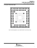
Reserved
NA
B11,
D6, D7,
D8, E4,
E5, E6,
E7, E8,
E9, F4,
F5, F8,
F9, G4,
G5,G8,
G9, H4,
H5, H6,
H7, H8,
H9, J5,
J6, J7,
J8, L2,
L11
BGA package unused balls. Connection to DV
SS
/AV
SS
recommended.
NOTE 1: It is recommended to connect GND externally to DVss.
Содержание MSP430FG47x
Страница 91: ......

