background image

MSP430FG47x

MIXED SIGNAL MICROCONTROLLER

SLAS580D -- OCTOBER 2008 -- REVISED MARCH 2011

31

POST OFFICE BOX 655303

DALLAS, TEXAS 75265

electrical characteristics over recommended operating free-air temperature (unless otherwise

noted) (continued)
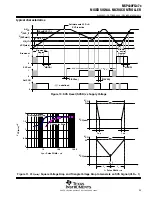
typical characteristics (continued)

VCC(min)

VCC
3 V

tpw

0

0.5

1

1.5

2

0.001

1

1000

Typical Conditions

1 ns

1 ns

t

pw

-- Pulse Width --

s

V

CC(min)

--

V

t

pw

-- Pulse Width --

s

V

CC

= 3 V

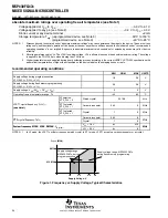
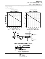
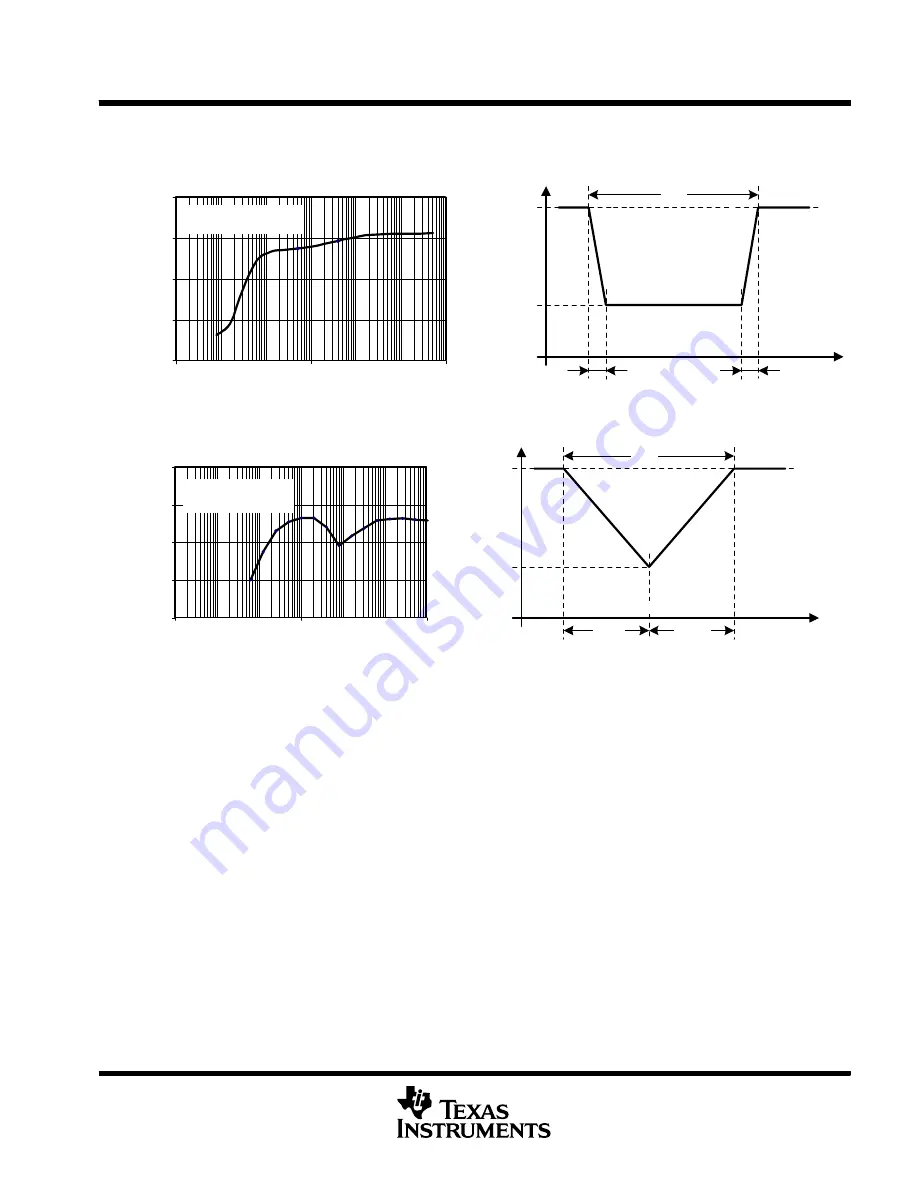
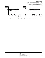
Figure 8. V

(CC)min

Level With a Square Voltage Drop to Generate a POR/Brownout Signal

VCC

0

0.5

1

1.5

2

VCC(min)

t pw

t

pw

-- Pulse Width --

s

V

CC(min)

--

V

3 V

0.001

1

1000

t

f

t

r

t

pw

-- Pulse Width --

s

t

f =

t

r

Typical Conditions

V

CC

= 3 V

Figure 9. V

CC(min)

Level With a Triangle Voltage Drop to Generate a POR/Brownout Signal

Содержание MSP430FG47x

Страница 1: ...aturing different sets of peripherals targeted for various applications The architecture combined with five low power modes is optimized to achieve extended battery life in portable measurement applications The device features a powerful 16 bit RISC CPU 16 bit registers and constant generators that contribute to maximum code efficiency The digitally controlled oscillator DCO allows wake up from lo...

Страница 2: ...tion Addendum at the end of this document or see the TI web site at www ti com Package drawings thermal data and symbolization are available at www ti com packaging DEVELOPMENT TOOL SUPPORT All MSP430 microcontrollers include an Embedded Emulation Module EEM allowing advanced debugging and programming through easy to use development tools Recommended hardware options include the following D Debugg...

Страница 3: ...430xG47x Terminal Functions table A1 B1 C1 D1 E1 F1 G1 H1 J1 K1 L1 M1 A2 B2 C2 D2 E2 F2 G2 H2 J2 K2 L2 M2 A3 A4 A5 A6 A7 A8 A9 A10 E5 E6 E7 E8 A11 B11 C11 D11 E11 F11 G11 H11 J11 K11 L11 M11 A12 B12 C12 D12 E12 F12 G12 H12 J12 K12 L12 M12 M3 M4 M5 M6 M7 M8 M9 M10 L3 L4 L5 L6 L7 L8 L9 L10 B3 B4 B5 B6 B7 B8 B9 B10 H5 H6 H7 H8 D4 D5 D6 D7 D8 D9 E4 F4 G4 H4 F5 G5 F8 G8 E9 F9 G9 H9 C3 J4 J5 J6 J7 J8 J9...

Страница 4: ...A0FB P6 0 A0 OA0O RST NMI TCK TMS TDI TCLK TDO TDI P5 6 LCDREF R13 78 77 76 75 74 73 72 71 70 69 68 67 66 65 58 57 56 55 54 53 52 51 50 49 48 47 46 45 1 2 3 4 5 6 7 8 9 10 11 12 13 14 15 16 21 22 23 24 25 26 27 28 29 30 31 32 33 34 35 36 64 63 62 61 37 S23 38 39 40 44 43 42 41 P4 4 S7 P4 3 S8 P4 2 S9 P4 1 S10 17 18 19 20 P3 7 S31 P3 6 S30 P3 5 S29 P3 4 S28 P3 3 UCB0CLK UCA0STE S24 S25 COM0 P5 2 CO...

Страница 5: ...6 Registers EEM JTAG Interface OA0 OA1 2 OpAmps Basic Timer Real Time Clock LCD_A 128 Segments 1 2 3 4 Mux Timer_B3 3 CC Registers Shadow Reg SD16_A with Buffer 1 Channel Sigma Delta A D Converter Comparator _A AVCC AVSS P1 x P2 x 2x8 P3 x P4 x P5 x P6 x 4x8 SMCLK ACLK MDB MAB DAC12 12 Bit 2 Channels Voltage Out Ports P1 P2 2x8 I O Interrupt capability XIN XT2IN 2 2 XOUT XT2OUT RAM 2kB 2kB 2kB Fla...

Страница 6: ...pin Timer_A capture CCI1A input compare Out1 output SD16 negative analog input A4 OA0 analog input I3 P1 3 TBOUTH SVSOUT A4 OA1I3 SW1C 55 D12 I O General purpose digital I O pin Timer_A capture CCI2A input compare Out2 output switch all PWM digital output ports to high impedance Timer_B TB0 to TB2 SVS comparator output SD16 positive analog input A4 OA1 analog input I3 P1 4 TBCLK SMCLK A3 OA1I0 DAC...

Страница 7: ...digital I O pin USCI B0 slave in master out in SPI mode SDA I2C data in I2C mode LCD segment output 26 P3 2 UCB0SOMI UCB0SCL S27 43 K11 I O General purpose digital I O pin USCI B0 slave out master in in SPI mode SCL I2C clock in I2C mode LCD segment output 27 P3 3 UCB0CLK UCA0STE 44 K12 I O General purpose digital I O USCI B0 clock input output USCI A0 slave transmit enable P3 4 S28 45 J11 I O Gen...

Страница 8: ...10 I O General purpose digital I O pin External LCD reference voltage input input port of the third most positive analog LCD level V3 or V2 P5 7 R03 40 M11 I O General purpose digital I O pin input port of the fourth most positive analog LCD level V1 P6 0 A0 OA0O 67 B8 I O General purpose digital I O pin SD16 positive analog input A0 OA0 output P6 1 A0 OA0FB 66 B9 I O General purpose digital I O p...

Страница 9: ...oscillator See Note NO TAG VREF 60 A12 O Input for an external reference voltage internal reference voltage output RST NMI 74 B5 I Reset input nonmaskable interrupt input port or bootstrap loader start in flash devices TCK 73 A5 I Test clock JTAG TCK is the clock input port for device programming test and bootstrap loader start TDI TCLK 71 A6 I Test data input or test clock input The device protec...

Страница 10: ...of the CPU clock Four of the registers R0 to R3 are dedicated as program counter stack pointer status register and constant generator respectively The remaining registers are general purpose registers Peripherals are connected to the CPU using data address and control buses and can be handled with all instructions instruction set The instruction set consists of 51 instructions with three formats a...

Страница 11: ...ctive mode AM All clocks are active D Low power mode 0 LPM0 CPU is disabled ACLK and SMCLK remain active FLL loop control remains active D Low power mode 1 LPM1 CPU is disabled ACLK and SMCLK remain active FLL loop control is disabled D Low power mode 2 LPM2 CPU is disabled MCLK FLL loop control and DCOCLK are disabled DCO s dc generator remains enabled ACLK remains active D Low power mode 3 LPM3 ...

Страница 12: ... 11 Watchdog Timer WDTIFG Maskable 0xFFF4 10 USCI_A0 USCI_B0 receive USCI_B0 I2C status UCA0RXIFG UCB0RXIFG see Notes 1 and 5 Maskable 0xFFF2 9 USCI_A0 USCI_B0 transmit USCI_B0 I2C receive transmit UCA0TXIFG UCB0TXIFG see Note 1 and 6 Maskable 0xFFF0 8 SD16_A SD16CCTLx SD16OVIFG SD16CCTLx SD16IFG see Notes 1 and 2 Maskable 0xFFEE 7 Timer_A3 TACCR0 CCIFG0 see Note 2 Maskable 0xFFEC 6 Timer_A3 TACCR...

Страница 13: ...Address 7 6 5 4 3 2 1 0 00h ACCVIE NMIIE OFIE WDTIE rw 0 rw 0 rw 0 rw 0 WDTIE Watchdog timer interrupt enable Inactive if watchdog mode is selected Active if watchdog timer is configured in interval timer mode OFIE Oscillator fault enable NMIIE Non maskable interrupt enable ACCVIE Flash access violation interrupt enable Address 7 6 5 4 3 2 1 0 01h BTIE UCB0TXIE UCB0RXIE UCA0TXIE UCA0RXIE rw 0 rw 0...

Страница 14: ...errupt flag Set on a reset condition at RST NMI pin in reset mode Reset on VCC power up PORIFG Power on interrupt flag Set on VCC power up NMIIFG Set via RST NMI pin Address 7 6 5 4 3 2 1 0 03h BTIFG UCB0 TXIFG UCB0 RXIFG UCA0 TXIFG UCA0 RXIFG rw 0 rw 1 rw 0 rw 1 rw 0 UCA0RXIFG USCI_A0 receive interrupt flag UCA0TXIFG USCI_A0 transmit interrupt flag UCB0RXIFG USCI_B0 receive interrupt flag UCB0TXI...

Страница 15: ...word For complete description of the features of the BSL and its implementation see the application report Features of the MSP430 Bootstrap Loader literature number SLAA089 BSL FUNCTION PN PACKAGE PINS ZQW PACKAGE PINS Data Transmit 58 P1 0 C11 P1 0 Data Receive 57 P1 1 C12 P1 1 flash memory Flash The flash memory can be programmed via the JTAG port the bootstrap loader or in system by the CPU The...

Страница 16: ...om a 32768 Hz watch crystal or a high frequency crystal D Main clock MCLK the system clock used by the CPU D Sub Main clock SMCLK the sub system clock used by the peripheral modules D ACLK n the buffered output of ACLK ACLK 2 ACLK 4 or ACLK 8 brownout supply voltage supervisor The brownout circuit is implemented to provide the proper internal reset signal to the device during power on and power of...

Страница 17: ...ent drive information Common and segment signals are generated as defined by the mode Static 2 MUX 3 MUX and 4 MUX LCDs are supported by this peripheral The module can provide a LCD voltage independent of the supply voltage via an integrated charge pump Furthermore it is possible to control the level of the LCD voltage and thus contrast in software Timer_A3 Timer_A3 is a 16 bit timer counter with ...

Страница 18: ...0 CCI0A P2 1 3 C1 P2 1 3 C1 TB0 CCI0B CCR0 TB0 VSS GND CCR0 TB0 VCC VCC P2 2 2 B1 TB1 CCI1A P2 2 2 B1 P2 2 2 B1 TB1 CCI1B CCR1 TB1 VSS GND CCR1 TB1 VCC VCC P2 3 77 B4 TB2 CCI2A P2 3 77 B4 ACLK internal CCI2B CCR2 TB2 VSS GND CCR2 TB2 VCC VCC NOTE 1 The inversion of TBCLK is done inside the module universal serial communication interfaces USCIs USCI_A0 USCI_B0 The USCI module is used for serial dat...

Страница 19: ...ion OA The MSP430FG47x has two configurable low current general purpose operational amplifiers Each OA input and output terminal is software selectable and offer a flexible choice of connections for various applications The OA op amps primarily support front end analog signal conditioning prior to analog to digital conversion OA0 SIGNAL CONNECTIONS INPUT PIN NUMBER DEVICE INPUT MODULE MODULE MODUL...

Страница 20: ...mer_A control TACTL 0160h Timer_A interrupt vector TAIV 012Eh Flash Flash control 4 Fl h l FCTL4 FCTL 01BEh Ch Flash control 3 Flash control 2 FCTL3 FCTL2 012Ch 012Ah Flash control 2 Flash control 1 FCTL2 FCTL1 012Ah 0128h DAC12 DAC12_1 data DAC12_1DAT 01CAh DAC12 DAC12_1 data DAC12_1 control DAC12_1DAT DAC12_1CTL 01CAh 01C2h DAC12_1 control DAC12_0 data DAC12_1CTL DAC12_0DAT 01C2h 01C8h _ DAC12_0...

Страница 21: ... 0x0062 USCI A0 control 1 UCA0CTL1 0x0061 USCI A0 control 0 UCA0CTL0 0x0060 USCI A0 IrDA receive control UCA0IRRCTL 0x005F USCI A0 IrDA transmit control UCA0IRTCTL 0x005E USCI B0 transmit buffer UCB0TXBUF 0x006F USCI B0 receive buffer UCB0RXBUF 0x006E USCI B0 status UCB0STAT 0x006D USCI B0 I2C Interrupt enable UCB0CIE 0x006C USCI B0 baud rate control 1 UCB0BR1 0x006B USCI B0 baud rate control 0 UC...

Страница 22: ...T1 RTCNT4 RTCDOW RTCNT3 RTCHOUR RTCNT2 RTCMIN RTCNT1 RTCSEC RTCCTL BTCTL 04Fh 04Eh 04Dh 04Ch 047h 046h 045h 044h 043h 042h 041h 040h Port P6 Port P6 selection P6SEL 037h Port P6 direction P6DIR 036h Port P6 output P6OUT 035h Port P6 input P6IN 034h Port P5 Port P5 selection P5SEL 033h Port P5 direction P5DIR 032h Port P5 output P5OUT 031h Port P5 input P5IN 030h Port P4 Port P4 selection P4SEL 01F...

Страница 23: ... Port P1 interrupt enable P1IE 025h Port P1 interrupt edge select P1IES 024h Port P1 interrupt flag P1IFG 023h Port P1 direction P1DIR 022h Port P1 output P1OUT 021h Port P1 input P1IN 020h Special functions SFR interrupt flag 2 IFG2 003h Special functions SFR interrupt flag 2 SFR i t t fl 1 IFG2 IFG1 003h 002h SFR interrupt flag 1 IFG1 002h p g SFR interrupt enable 2 IE2 001h SFR interrupt enable...

Страница 24: ...plied during board soldering process according to the current JEDEC J STD 020 specification with peak reflow temperatures not higher than classified on the device label on the shipping boxes or reels recommended operating conditions MIN NOM MAX UNITS Supply voltage during program execution VCC AVCC DVCC VCC 1 8 3 6 V Supply voltage during flash memory programming VCC AVCC DVCC VCC 2 2 3 6 V Supply...

Страница 25: ...DCPEN 0 static mode fLCD f ACLK 32 TA 25 C 3 V 1 2 2 0 LCD ACLK see Note 2 and Note 3 TA 60 C 3 V 1 4 2 2 TA 85 C 2 7 4 5 Low power mode LPM3 TA 40 C 1 0 3 0 Low power mode LPM3 f MCLK f SMCLK 0 MHz TA 25 C 2 2 V 1 1 3 2 I f MCLK f SMCLK 0 MHz f ACLK 32 768 Hz SCG0 1 Basic Timer1 enabled ACLK selected TA 85 C 2 2 V 3 5 6 0 A I LPM3 Basic Timer1 enabled ACLK selected LCD A enabled LCDCPEN 0 TA 40 C...

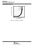
Страница 26: ...655303 DALLAS TEXAS 75265 typical characteristics LPM4 current 0 0 0 2 0 4 0 6 0 8 1 0 1 2 1 4 1 6 1 8 2 0 40 0 20 0 0 0 20 0 40 0 60 0 80 0 100 0 120 0 TA Temperature C Vcc 3 6 V TA Temperature C Vcc 1 8 V Vcc 3 0 V Vcc 2 2 V I LPM4 Low Power Mode 4 Current A Figure 2 ILPM4 LPM4 Current vs Temperature ...

Страница 27: ...nal trigger signal 2 2 V 62 ns t int External interrupt timing Port P1 P2 P1 x to P2 x external trigger signal for the interrupt flag see Note 1 3 V 50 ns t Timer A capture timing TA0 TA1 TA2 2 2 V 62 ns t cap Timer_A capture timing TA0 TA1 TA2 3 V 50 ns f Timer_A clock frequency externally TACLK INCLK t t 2 2 V 8 MHz f TAext Timer_A clock frequency externally applied to pin TACLK INCLK t H t L 3 ...

Страница 28: ... Low level output voltage IOL max 6 mA VCC 2 2 V See Note 2 VSS VSS 0 6 V VOL Low level output voltage IOL max 1 5 mA VCC 3 V See Note 1 VSS VSS 0 25 V IOL max 6 mA VCC 3 V See Note 2 VSS VSS 0 6 NOTES 1 The maximum total current IOH max and IOL max for all outputs combined should not exceed 12 mA to satisfy the maximum specified voltage drop 2 The maximum total current IOH max and IOL max for all...

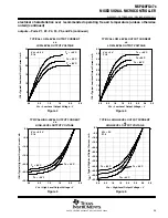
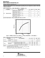
Страница 29: ...tput Voltage V 0 5 10 15 20 25 30 35 40 45 50 0 0 0 5 1 0 1 5 2 0 2 5 3 0 3 5 VCC 3 V P1 0 TYPICAL LOW LEVEL OUTPUT CURRENT vs LOW LEVEL OUTPUT VOLTAGE TA 25 C TA 85 C OL I Typical Low level Output Current mA TA 40 C Figure 5 VOH High Level Output Voltage V 30 0 25 0 20 0 15 0 10 0 5 0 0 0 0 0 0 5 1 0 1 5 2 0 2 5 VCC 2 2 V P1 0 TYPICAL HIGH LEVEL OUTPUT CURRENT vs HIGH LEVEL OUTPUT VOLTAGE TA 25 C...

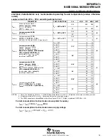
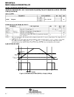
Страница 30: ... 7 through Figure 9 1 71 V Vhys B_IT see Note 2 dVCC dt 3 V s see Figure 7 mV t reset Pulse length needed at RST NMI pin to accepted reset internally VCC 2 2 V 3 V 2 s NOTES 1 The current consumption of the brownout module is already included in the ICC current consumption data The voltage level V B_IT Vhys B_IT is 1 8V 2 During power up the CPU begins code execution following a period of td BOR a...

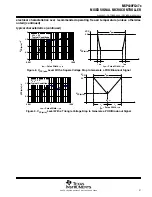
Страница 31: ...ristics continued VCC min VCC 3 V tpw 0 0 5 1 1 5 2 0 001 1 1000 Typical Conditions 1 ns 1 ns tpw Pulse Width s V CC min V tpw Pulse Width s VCC 3 V Figure 8 V CC min Level With a Square Voltage Drop to Generate a POR Brownout Signal VCC 0 0 5 1 1 5 2 VCC min tpw tpw Pulse Width s V CC min V 3 V 0 001 1 1000 tf tr tpw Pulse Width s tf tr Typical Conditions VCC 3 V Figure 9 VCC min Level With a Tri...

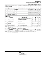
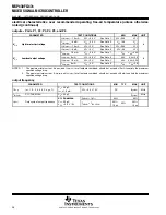
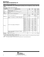
Страница 32: ... 4 20 mV VLD 1 1 8 1 9 2 05 VLD 2 1 94 2 1 2 25 VLD 3 2 05 2 2 2 37 VLD 4 2 14 2 3 2 48 VLD 5 2 24 2 4 2 6 VLD 6 2 33 2 5 2 71 V dt 3 V s see Figure 10 and Figure 11 VLD 7 2 46 2 65 2 86 V SVS IT VCC dt 3 V s see Figure 10 and Figure 11 VLD 8 2 58 2 8 3 V V SVS_IT VLD 9 2 69 2 9 3 13 V VLD 10 2 83 3 05 3 29 VLD 11 2 94 3 2 3 42 VLD 12 3 11 3 35 3 61 VLD 13 3 24 3 5 3 76 VLD 14 3 43 3 7 3 99 VCC dt...

Страница 33: ...fined Vhys SVS_IT 0 1 td BOR Brownout 0 1 td SVSon td BOR 0 1 Set POR Brown out Region SVS Circuit is Active From VLD to VCC V B_IT SVS out Vhys B_IT Figure 10 SVS Reset SVSR vs Supply Voltage 0 0 5 1 1 5 2 VCC VCC 1 ns 1 ns VCC min tpw tpw Pulse Width s V CC min V 3 V 1 10 1000 tf tr t Pulse Width s 100 tpw 3 V tf tr Rectangular Drop Triangular Drop VCC min Figure 11 VCC min Square Voltage Drop a...

Страница 34: ...8 FN 4 0 FN 3 1 FN 2 DCOPLUS 1 see Note 1 2 2 V 9 15 5 25 MH f DCO27 FN_8 FN_4 0 FN_3 1 FN_2 x DCOPLUS 1 see Note 1 3 V 10 3 17 9 28 5 MHz f FN 8 0 FN 4 1 FN 3 FN 2 DCOPLUS 1 2 2 V 1 8 2 8 4 2 MH f DCO2 FN_8 0 FN_4 1 FN_3 FN_2 x DCOPLUS 1 3 V 2 1 3 4 5 2 MHz f FN 8 0 FN 4 1 FN 3 FN 2 DCOPLUS 1 see Note 1 2 2 V 13 5 21 5 33 MH f DCO27 FN_8 0 FN_4 1 FN_3 FN_2 x DCOPLUS 1 see Note 1 3 V 16 26 6 41 MH...

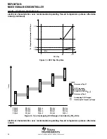
Страница 35: ...LAS580D OCTOBER 2008 REVISED MARCH 2011 35 POST OFFICE BOX 655303 DALLAS TEXAS 75265 TA C VCC V f DCO f DCO20 C f DCO f DCO3V 1 8 3 0 2 4 3 6 1 0 20 60 40 85 1 0 0 20 40 0 Figure 12 DCO Frequency vs Supply Voltage VCC and vs Ambient Temperature ...

Страница 36: ... Max 1 07 1 06 Figure 13 DCO Tap Step Size DCO Frequency Adjusted by Bits 29 to 25 in SCFI1 N DCO FN_2 0 FN_3 0 FN_4 0 FN_8 0 FN_2 1 FN_3 0 FN_4 0 FN_8 0 FN_2 x FN_3 1 FN_4 0 FN_8 0 FN_2 x FN_3 x FN_4 1 FN_8 0 FN_2 x FN_3 x FN_4 x FN_8 1 Legend Tolerance at Tap 27 Tolerance at Tap 2 Overlapping DCO Ranges Uninterrupted Frequency Range f DCO Figure 14 Five Overlapping DCO Ranges Controlled by FN_x ...

Страница 37: ... pF per pin Since the PCB adds additional capacitance it is recommended to verify the correct load by measuring the ACLK frequency For a correct setup the effective load capacitance should always match the specification of the used crystal 2 Measured with logic level input frequency but also applies to operation with crystals 3 Frequencies below the MIN specification set the fault flag frequencies...

Страница 38: ...CLK frequency For a correct setup the effective load capacitance should always match the specification of the used crystal 2 Requires external capacitors at both terminals Values are specified by crystal manufacturers crystal oscillator XT2 high frequency modes PARAMETER TEST CONDITIONS VCC MIN TYP MAX UNIT fXT2 XT2 oscillator crystal frequency Ceramic resonator 1 8 V to 3 6 V 0 45 8 MHz fXT2 XT2 ...

Страница 39: ... 25 C 2 2 V 3 8 A fLCD LCD frequency 1 1 kHz VLCD LCD voltage VLCDx 0000 VCC V VLCD LCD voltage VLCDx 0001 2 60 V VLCD LCD voltage VLCDx 0010 2 66 V VLCD LCD voltage VLCDx 0011 2 72 V VLCD LCD voltage VLCDx 0100 2 78 V VLCD LCD voltage VLCDx 0101 2 84 V VLCD LCD voltage VLCDx 0110 2 90 V VLCD LCD voltage VLCDx 0111 2 96 V VLCD LCD voltage VLCDx 1000 3 02 V VLCD LCD voltage VLCDx 1001 3 08 V VLCD L...

Страница 40: ...1 VCC 2 2 V 390 480 540 mV V RefVT See Figure 15 and Figure 16 No load at P1 6 CA0 and P1 7 CA1 TA 85 C VCC 3 V 400 490 550 mV VIC Common mode input voltage range CAON 1 VCC 2 2 V 3 V 0 VCC 1 V Vp VS Offset voltage See Note 2 VCC 2 2 V 3 V 30 30 mV Vhys Input hysteresis CAON 1 VCC 2 2 V 3 V 0 0 7 1 4 mV TA 25 C VCC 2 2 V 80 165 300 ns t see Note 3 TA 25 C Overdrive 10 mV without filter CAF 0 VCC 3...

Страница 41: ...5 95 VCC 3 V Figure 15 V RefVT vs Temperature V REF Reference Voltage mV Typical REFERENCE VOLTAGE vs FREE AIR TEMPERATURE Figure 16 V RefVT vs Temperature TA Free Air Temperature C 400 450 500 550 600 650 45 25 5 15 35 55 75 95 VCC 2 2 V Typical REFERENCE VOLTAGE vs FREE AIR TEMPERATURE V REF Reference Voltage mV _ CAON 0 1 V 0 1 CAF Low Pass Filter 2 s To Internal Modules Set CAIFG Flag CAOUT V ...

Страница 42: ...C MIN TYP MAX UNIT V Absolute input SD16BUFx 00 AVSS 0 1V AVCC V VI Absolute input voltage range SD16BUFx 00 AVSS 0 2V AVCC 1 2 V V V Common mode SD16BUFx 00 AVSS 0 1V AVCC V VIC Common mode input voltage range SD16BUFx 00 AVSS 0 2V AVCC 1 2 V V V Differential full scale input voltage Bipolar mode SD16UNI 0 VREF 2GAIN VREF 2GAIN mV VID FSR scale input voltage range Unipolar mode SD16UNI 1 0 VREF 2...

Страница 43: ... VCC MIN TYP MAX UNIT SD16GAINx 1 Signal Amplitude 500mV 3 V 83 5 85 SD16GAINx 2 Signal Amplitude 250mV 3 V 81 5 84 SINAD Signal to noise SD16GAINx 4 Signal Amplitude 125mV fIN 50Hz 3 V 76 79 5 dB SINAD Signal to noise distortion ratio SD16GAINx 8 Signal Amplitude 62mV fIN 50Hz 100Hz 3 V 73 76 5 dB SD16GAINx 16 Signal Amplitude 31mV 3 V 69 73 SD16GAINx 32 Signal Amplitude 15mV 3 V 62 69 SD16GAINx ...

Страница 44: ...95 0 100 0 10 00 100 00 1000 00 SINAD dB Figure 19 SINAD performance over OSR fSD16 1MHz SD16REFON 1 SD16GAINx 1 SD16_A temperature sensor and built in VCC sense PARAMETER TEST CONDITIONS VCC MIN TYP MAX UNIT TCSensor Sensor temperature coefficient See Note 1 1 18 1 32 1 46 mV K VOffset sensor Sensor offset voltage See Note 1 100 100 mV S t t lt Temperature sensor voltage at TA 85 C 3 V 435 475 51...

Страница 45: ...FON 1 SD16VMIDON 0 3 V 100 uV V NOTES 1 Calculated using the box method MAX 40 85_C MIN 40 85_C MIN 40 85_C 85C 40_C 2 There is no capacitance required on VREF However a capacitance of at least 100nF is recommended to reduce any reference voltage noise SD16_A reference output buffer PARAMETER TEST CONDITIONS VCC MIN TYP MAX UNIT VREF BUF Reference buffer output voltage SD16REFON 1 SD16VMIDON 1 3 V...

Страница 46: ...C12_xDAT 0800h VREF DAC12 AVCC 2 2 V 3 V 50 110 A IDD Supply current see Notes 1 and 2 DAC12AMPx 5 DAC12IR 1 DAC12_xDAT 0800h VREF DAC12 AVCC 2 2 V 3 V 200 440 A DAC12AMPx 7 DAC12IR 1 DAC12_xDAT 0800h VREF DAC12 AVCC 2 2 V 3 V 700 1500 PSRR Power supply rejection ratio see Notes 3 and 4 DAC12_xDAT 800h VREF DAC12 1 2 V AVCC 100 mV 2 7 V 70 dB NOTES 1 No load at the output pin assuming that the con...

Страница 47: ...cient see Note 1 2 7 V 30 V C EG Gain error see Note 1 VREF DAC12 1 2 V 2 7 V 3 50 FSR dE G dT Gain temperature coefficient see Note 1 2 7 V 10 ppm of FSR C Time for offset calibration DAC12AMPx 2 2 7 V 100 tOffset Cal Time for offset calibration see Note 3 DAC12AMPx 3 5 2 7 V 32 ms tOffset_Cal see Note 3 DAC12AMPx 4 6 7 2 7 V 6 ms NOTES 1 Parameters calculated from the best fit curve from 0x0A to...

Страница 48: ...ity specifications continued DAC12_xDAT Digital Code 4 3 2 1 0 1 2 3 4 0 512 1024 1536 2048 2560 3072 3584 VCC 2 2 V VREF 1 2 V DAC12AMPx 7 DAC12IR 1 TYPICAL INL ERROR vs DIGITAL INPUT DATA 4095 INL Integral Nonlinearity Error LSB DAC12_xDAT Digital Code 2 0 1 5 1 0 0 5 0 0 0 5 1 0 1 5 2 0 0 512 1024 1536 2048 2560 3072 3584 VCC 2 2 V VREF 1 2 V DAC12AMPx 7 DAC12IR 1 TYPICAL DNL ERROR vs DIGITAL I...

Страница 49: ...d 3 k VREF DAC12 AVCC DAC12_xDAT 0h DAC12IR 1 DAC12AMPx 7 2 2 V 3 V 0 0 1 V RLoad 3 k VREF DAC12 AVCC DAC12_xDAT 0FFFh DAC12IR 1 DAC12AMPx 7 2 2 V 3 V AVCC 0 13 AVCC CL DAC12 Max DAC12 load capacitance 2 2 V 3 V 100 pF I Max DAC12 load 2 2V 0 5 0 5 mA IL DAC12 Max DAC12 load current 3V 1 0 1 0 mA RLoad 3 k VO P DAC12 0 3 V DAC12AMPx 2 DAC12_xDAT 0h 2 2 V 3 V 150 250 RO P DAC12 Output resistance se...

Страница 50: ...T CONDITIONS VCC MIN TYP MAX UNIT DAC12 DAC12_xDAT 800h DAC12AMPx 0 2 3 4 2 2 V 3 V 60 120 tON DAC12 on time DAC12_xDAT 800h ErrorV O 0 5 LSB DAC12AMPx 0 5 6 2 2 V 3 V 15 30 s tON on time ErrorV O 0 5 LSB see Note 1 Figure 24 DAC12AMPx 0 7 2 2 V 3 V 6 12 s Settling DAC12 xDAT DAC12AMPx 2 2 2 V 3 V 100 200 tS FS Settling time full scale DAC12_xDAT 80h F7Fh 80h DAC12AMPx 3 5 2 2 V 3 V 40 80 s tS FS ...

Страница 51: ...namic specifications continued TA 25 C unless otherwise noted PARAMETER TEST CONDITIONS VCC MIN MAX UNIT 3 dB bandwidth DAC12AMPx 2 3 4 DAC12SREFx 2 DAC12IR 1 DAC12_xDAT 800h 2 2 V 3 V 40 BW 3dB 3 dB bandwidth VDC 1 5 V VAC 0 1VPP DAC12AMPx 5 6 DAC12SREFx 2 DAC12IR 1 DAC12_xDAT 800h 2 2 V 3 V 180 kHz AC PP see Figure 26 DAC12AMPx 7 DAC12SREFx 2 DAC12IR 1 DAC12_xDAT 800h 2 2 V 3 V 550 NOTES 1 RLOAD...

Страница 52: ... nA IIkg Input leakage current see Notes 1 and 2 TA 55 to 85_C 2 2 V 3 V 20 5 20 nA Fast Mode 50 Medium Mode fV I P 1 kHz 80 V Voltage noise densit I P Slow Mode fV I P 1 kHz 140 nV H Vn Voltage noise density I P Fast Mode 30 nV Hz Medium Mode fV I P 10 kHz 50 Slow Mode fV I P 10 kHz 65 VIO Offset voltage I P 2 2 V 3 V 10 mV Offset temperature drift I P see Note 3 2 2 V 3 V 10 V C Offset voltage d...

Страница 53: ...F 60 deg Gain margin CL 50 pF 20 dB Noninverting Fast Mode RL 47 k CL 50 pF 2 2 GBW Gain bandwidth product see Figure 27 and Figure 28 Noninverting Medium Mode RL 300 k CL 50pF 2 2 V 3 V 1 4 MHz see Figure 27 and Figure 28 Non inverting Slow Mode RL 300 k CL 50pF 0 5 ten on Enable time on ton Noninverting Gain 1 2 2 V 3 V 10 20 s ten off Enable time off 2 2 V 3 V 1 s Figure 27 Input Frequency kHz ...

Страница 54: ... current see Note 1 TA 55 C to 85 C 50 nA IIN Input current Input switched to ON 0 100 A RON On resistance IIN 100 A 1 k NOTES 1 ESD damage can degrade input current leakage typical characteristics Figure 29 500 0 750 0 1000 0 1250 0 1500 0 1750 0 2000 0 2250 0 2500 0 2750 0 3000 0 0 0 0 4 0 8 1 2 1 6 2 0 2 4 2 8 3 2 3 6 VCC 3 6 V Typical VCC 2 7 V VCC 3 V VCC 2 2 V RON vs VCOM VCOM Common Mode In...

Страница 55: ...UNIT f Timer A clock frequency Internal SMCLK ACLK External TACLK INCLK 2 2 V 8 MHz fTA Timer_A clock frequency External TACLK INCLK Duty cycle 50 10 3 V 10 MHz tTA cap Timer_A capture timing TA0 TA1 TA2 2 2 V 3 V 20 ns Timer_B PARAMETER TEST CONDITIONS VCC MIN MAX UNIT f Timer B clock frequency Internal SMCLK ACLK External TBCLK 2 2 V 8 MHz fTB Timer_B clock frequency External TBCLK Duty cycle 50...

Страница 56: ...0 ns tHD MI SOMI input data hold time 3 V 0 ns t SIMO output data valid time UCLK edge to SIMO valid C 20 pF 2 2 V 30 ns tVALID MO SIMO output data valid time UCLK edge to SIMO valid CL 20 pF 3 V 20 ns NOTE fUCxCLK 1 2tLO HI with tLO HI max tVALID MO USCI tSU SI Slave tSU MI USCI tVALID SO Slave For the slave s parameters tSU SI Slave and tVALID SO Slave refer to the SPI parameters of the attached...

Страница 57: ...racteristics over recommended ranges of supply voltage and operating free air temperature unless otherwise noted continued UCLK CKPL 0 CKPL 1 SIMO 1 fUCxCLK tLO HI tLO HI SOMI tSU MI tHD MI tVALID MO Figure 31 SPI Master Mode CKPH 0 UCLK CKPL 0 CKPL 1 SIMO 1 fUCxCLK tLO HI tLO HI SOMI tSU MI tHD MI tVALID MO Figure 32 SPI Master Mode CKPH 1 ...

Страница 58: ...supply voltage and operating free air temperature unless otherwise noted continued STE UCLK CKPL 0 CKPL 1 SOMI tSTE ACC tSTE DIS 1 fUCxCLK tLO HI tLO HI SIMO tSU SI tHD SI tVALID SO tSTE LEAD tSTE LAG Figure 33 SPI Slave Mode CKPH 0 STE UCLK CKPL 0 CKPL 1 tSTE LEAD tSTE LAG tSTE ACC tSTE DIS tLO HI tLO HI tSU SI tHD SI tVALID SO SOMI SIMO 1 fUCxCLK Figure 34 SPI Slave Mode CKPH 1 ...

Страница 59: ... fSCL SCL clock frequency 2 2 V 3 V 0 400 kHz t Hold time repeated START fSCL 100kHz 2 2 V 3 V 4 0 s tHD STA Hold time repeated START fSCL 100kHz 2 2 V 3 V 0 6 s t Set p time for a repeated START fSCL 100kHz 2 2 V 3 V 4 7 s tSU STA Setup time for a repeated START fSCL 100kHz 2 2 V 3 V 0 6 s tHD DAT Data hold time 2 2 V 3 V 0 ns tSU DAT Data setup time 2 2 V 3 V 250 ns tSU STO Setup time for STOP 2...

Страница 60: ...iting to a 64 byte flash block This parameter applies to all programming methods individual word byte write and block write modes 2 The mass erase duration generated by the flash timing generator is at least 11 1ms 5297x1 fFTG max 5297x1 476kHz To achieve the required cumulative mass erase time the Flash Controller s mass erase operation can be repeated until this time is met A worst case minimum ...

Страница 61: ...put 1 Output P1SEL 0 P1DIR 0 P1IN 0 P1IRQ 0 D EN Module X IN Module X OUT P1OUT 0 Interrupt Edge Select Q EN Set P1SEL 0 P1IES 0 P1IFG 0 P1IE 0 Pad Logic 1 0 0 1 1 0 P1SEL2 0 SWCTL1 SWCTL8 Bus Keeper EN OA0 CAPD 0 Port P1 P1 0 pin functions PIN NAME P1 X X FUNCTION CONTROL BITS SIGNALS PIN NAME P1 X X FUNCTION CAPD x P1DIR x P1SEL x P1SEL2 x P1 0 TA0 OA0RFB 0 P1 x I O 0 I 0 O 1 0 0 Timer_A3 CCI0A ...

Страница 62: ...put P1SEL 1 P1DIR 1 P1IN 1 P1IRQ 1 D EN Module X IN Module X OUT P1OUT 1 Interrupt Edge Select Q EN Set P1SEL 1 P1IES 1 P1IFG 1 P1IE 1 Pad Logic 1 0 0 1 1 0 P1SEL2 1 MCLK SWCTL1 SWCTL12 Bus Keeper EN OA1 CAPD 1 Port P1 P1 1 pin functions PIN NAME P1 X X FUNCTION CONTROL BITS SIGNALS PIN NAME P1 X X FUNCTION CAPD x P1DIR x P1SEL x P1SEL2 x P1 1 TA0 MCLK 1 P1 x I O 0 I 0 O 1 0 0 OA1RFB Timer_A3 CCI0...

Страница 63: ...R 2 P1IN 2 P1IRQ 2 D EN Module X IN Module X OUT P1OUT 2 Interrupt Edge Select Q EN Set P1SEL 2 P1IES 2 P1IFG 2 P1IE 2 Pad Logic 1 0 1 0 Bus Keeper EN SD16AE 2 INCH A4 0 1 DVSS OA0 CAPD 2 Port P1 P1 2 pin functions CONTROL BITS SIGNALS PIN NAME P1 X X FUNCTION CAPD x P1DIR x P1SEL x P1SEL2 x 0 OAN OA0 P1SEL2 x 0 SD16AE x P1 2 TA1 A4 OA0I3 2 P1 x I O 0 I 0 O 1 0 xx 0 Timer_A3 CCI1A 0 0 1 xx 0 Timer...

Страница 64: ...1SEL 3 P1DIR 3 P1IN 3 P1IRQ 3 D EN Module X IN Module X OUT P1OUT 3 Interrupt Edge Select Q EN Set P1SEL 3 P1IES 3 P1IFG 3 P1IE 3 Pad Logic 1 0 1 0 Bus Keeper EN SD16AE 3 INCH 4 A4 OA1 CAPD 3 Port P1 P1 3 pin functions CONTROL BITS SIGNALS PIN NAME P1 X X FUNCTION CAPD x P1DIR x P1SEL x P1SEL2 x 0 OAN OA1 P1SEL2 x 0 SD16AE x P1 3 TBOUTH 3 P1 x I O 0 I 0 O 1 0 xx 0 SVSOUT A4 OA1I3 TBOUTH 0 0 1 xx 0...

Страница 65: ... IN Module X OUT P1OUT 4 Pad Logic 1 0 1 0 Bus Keeper EN A3 DAC12_1OUT SD16AE 4 INCH 3 0 1 DVSS DAC12OPS OA1 P1IRQ 4 Interrupt Edge Select Q EN Set P1SEL 4 P1IES 4 P1IFG 4 P1IE 4 CAPD 4 Port P1 P1 4 pin functions CONTROL BITS SIGNALS PIN NAME P1 X X FUNCTION CAPD x P1DIR x P1SEL x P1SEL2 x 0 SD16AE x P1SEL2 x 0 OAP OA1 P1SEL2 x 0 DAC12OPS DAC12_1 P1 4TBCLK SMCLK 4 P1 x I O I 0 O 1 0 0 xx 0 A3 OA1I...

Страница 66: ...irection 0 Input 1 Output P1SEL 5 P1DIR 5 P1IN 5 P1IRQ 5 D EN Module X IN Module X OUT P1OUT 5 Interrupt Edge Select Q EN Set P1SEL 5 P1IES 5 P1IFG 5 P1IE 5 Pad Logic 1 0 1 0 Bus Keeper EN SD16AE 5 INCH 3 Ax CAPD 5 Port P1 P1 5 pin functions CONTROL BITS SIGNALS PIN NAME P1 X X FUNCTION CAPD x P1DIR x P1SEL x P1SEL2 x 0 SD16AE x P1 5 TACLK ACLK 5 P1 x I O 0 I 0 O 1 0 0 A3 TACLK 0 0 1 0 ACLK 0 1 1 ...

Страница 67: ...rt P1 pin schematic P1 6 input output with Schmitt trigger P1 6 CA0 A2 OA0I0 DAC0 Direction 0 Input 1 Output P1SEL 6 P1DIR 6 P1IN 6 D EN Module X IN 0 1 P1OUT 6 Pad Logic 1 0 1 0 Bus Keeper EN A2 DAC12OPS DAC12_0OUT SD16AE 6 INCH 2 CAPD 6 From Comparator_A To Comparator_A 0 1 DVSS OA0 P1IRQ 6 Interrupt Edge Select Q EN Set P1SEL 6 P1IES 6 P1IFG 6 P1IE 6 ...

Страница 68: ...Port P1 P1 6 pin functions CONTROL BITS SIGNALS PIN NAME P1 X X FUNCTION P1DIR x P1SEL x P1SEL2 x 0 CAPD x P1SEL2 x 0 SD16AE x P1SEL2 x 0 OAP OA0 P1SEL2 x 0 DAC12OPS DAC12_0 P1 6 CA0 A2 OA0I0 6 P1 x I O I 0 O 1 0 0 0 xx 0 DAC0 CA0 x x 1 or selected x xx x A2 x x x 1 xx x OA0I0 x x x x 00 x DAC0 x x x x xx 1 NOTES 1 x Don t care ...

Страница 69: ... 1 Output P1SEL 7 P1DIR 7 P1IN 7 D EN Module X IN 0 1 P1OUT 7 Pad Logic 1 0 1 0 Bus Keeper EN A2 SD16AE 7 INCH 2 CAPD 7 From Comparator_A To Comparator_A P1IRQ 7 Interrupt Edge Select Q EN Set P1SEL 7 P1IES 7 P1IFG 7 P1IE 7 Port P1 P1 7 pin functions CONTROL BITS SIGNALS PIN NAME P1 X X FUNCTION P1DIR x P1SEL x P1SEL2 x 0 CAPD x P1SEL2 x 0 SD16AE x P1 7 CA1 A2 7 P1 x I O I 0 O 1 0 0 0 CA1 x x 1 or...

Страница 70: ...Module X IN Module X OUT P2OUT x Interrupt Edge Select Q EN Set P2SEL x P2IES x P2IFG x P2IE x Pad Logic 1 0 1 0 Bus Keeper EN P2 0 TA2 S1 P2 1 TB0 S0 Segment Sx LCDS0 Port P2 P2 0 to P2 1 pin functions PIN NAME P2 X X FUNCTION CONTROL BITS SIGNALS PIN NAME P2 X X FUNCTION P2DIR x P2SEL x LCDS0 P2 0 TA2 S1 0 P2 x I O I 0 O 1 0 0 Timer_A3 CCI2A 0 1 0 Timer_A3 TA2 1 1 0 S1 x x 1 P2 1 TB0 S0 1 P2 x I...

Страница 71: ...Input 1 Output P2SEL x P2DIR x P2IN x P2IRQ x D EN Module X IN Module X OUT P2OUT x Interrupt Edge Select Q EN Set P2SEL x P2IES x P2IFG x P2IE x Pad Logic 1 0 1 0 P2 2 TB1 P2 3 TB2 Port P2 P2 2 to P2 3 pin functions PIN NAME P2 X X FUNCTION CONTROL BITS SIGNALS PIN NAME P2 X X FUNCTION P2DIR x P2SEL x P2 2 TB1 2 P2 x I O I 0 O 1 0 Timer_B3 CCI1A 0 1 Timer_B3 TB1 1 1 P2 3 TB2 3 P2 x I O I 0 O 1 0 ...

Страница 72: ...2OUT x Pad Logic 1 0 1 0 P2 4 UCA0TXD UCA0SIMO P2 5 UCA0RXD UCA0SOMI Module direction P2IRQ x Interrupt Edge Select Q EN Set P2SEL x P2IES x P2IFG x P2IE x Port P2 P2 4 and P2 5 pin functions PIN NAME P2 X X FUNCTION CONTROL BITS SIGNALS PIN NAME P2 X X FUNCTION P2DIR x P2SEL x P2 4 UCA0TXD 4 P2 x I O I 0 O 1 0 UCA0SIMO UCA0TXD UCA0SIMO see Notes 2 x 1 P2 5 UCA0RXD 5 P2 x I O I 0 O 1 0 UCA0SOMI UC...

Страница 73: ...3 Direction 0 Input 1 Output P2SEL x P2DIR x P2IN x 0 1 P2OUT x Pad Logic 1 0 1 0 Bus Keeper EN Segment Sy LCDS0 P2IRQ x Interrupt Edge Select Q EN Set P2SEL x P2IES x P2IFG x P2IE x Port P2 P2 6 and P2 7 pin functions PIN NAME P2 X X FUNCTION CONTROL BITS SIGNALS PIN NAME P2 X X FUNCTION P2DIR x P2SEL x LCDS0 P2 6 CAOUT S2 6 P2 x I O I 0 O 1 0 0 CAOUT 1 1 0 S2 x x 1 P2 7 S3 7 P2 x I O I 0 O 1 0 0...

Страница 74: ... P3IN x D EN Module X IN Module X OUT P3OUT x Pad Logic 1 0 1 0 P3 0 UCB0STE UCA0CLK P3 3 UCB0CLK UCA0STE Module direction Port P3 P3 0 and P3 3 pin functions PIN NAME P3 X X FUNCTION CONTROL BITS SIGNALS PIN NAME P3 X X FUNCTION P3DIR x P3SEL x P3 0 UCB0STE 0 P3 x I O I 0 O 1 0 UCA0CLK UCB0STE UCA0CLK see Note 2 x 1 P3 3 UCB0CLK 3 P3 x I O I 0 O 1 0 UCA0STE UCB0CLK UCA0STE see Note 2 x 1 NOTES 1 ...

Страница 75: ...SOMI UCB0SCL S27 Module direction Segment Sy LCDS24 Bus Keeper EN Port P3 P3 1 and P3 2 pin functions PIN NAME P3 X X FUNCTION CONTROL BITS SIGNALS PIN NAME P3 X X FUNCTION P3DIR x P3SEL x LCDS24 P3 1 UCB0SIMO 1 P3 x I O I 0 O 1 0 0 UCB0SDA S26 UCB0SIMO UCB0SDA see Notes 2 and 3 x 1 0 S26 x x 1 P3 2 UCB00SOMI 2 P3 x I O I 0 O 1 0 0 UCB0SCL S27 UCB0SOMI UCB0SCL see Notes 2 and 3 x 1 0 S27 x x 1 NOT...

Страница 76: ... P3 7 S31 Direction 0 Input 1 Output P3SEL x P3DIR x P3IN x Module X Out P3OUT x 1 0 1 0 Bus Keeper EN Pad Logic Segment Sy LCDS28 Port P3 P3 4 to P3 7 pin functions PIN NAME P3 X X FUNCTION CONTROL BITS SIGNALS PIN NAME P3 X X FUNCTION P3DIR x P3SEL x LCDS28 P3 4 S28 4 P3 x I O I 0 O 1 0 0 S28 x x 1 P3 5 S29 5 P3 x I O I 0 O 1 0 0 S29 x x 1 P3 6 S30 6 P3 x I O I 0 O 1 0 0 S30 x x 1 P3 7 S31 7 P3 ...

Страница 77: ...LCDS4 8 P4IN x Port P4 P4 0 and P4 7 pin functions PIN NAME P4 X X FUNCTION CONTROL BITS SIGNALS PIN NAME P4 X X FUNCTION P4DIR x P4SEL x LCDS4 8 P4 0 S11 0 P4 x I O I 0 O 1 0 0 LCDS8 S11 x x 1 LCDS8 P4 1 S10 1 P4 x I O I 0 O 1 0 0 LCDS8 S10 x x 1 LCDS8 P4 2 S9 2 P4 x I O I 0 O 1 0 0 LCDS8 S9 x x 1 LCDS8 P4 3 S8 3 P4 x I O I 0 O 1 0 0 LCDS8 S8 x x 1 LCDS8 P4 4 S7 4 P4 x I O I 0 O 1 0 0 LCDS4 S7 x ...

Страница 78: ... output with Schmitt trigger P5 0 S20 P5 1 S21 Direction 0 Input 1 Output P5SEL x P5DIR x P5IN x 0 1 P5OUT x 1 0 1 0 Bus Keeper EN Pad Logic Segment Sy LCDS20 Port P5 P5 0 and P5 1 pin functions PIN NAME P5 X X FUNCTION CONTROL BITS SIGNALS PIN NAME P5 X X FUNCTION P5DIR x P5SEL x LCDS20 P5 0 S20 0 P5 x I O I 0 O 1 0 0 S20 x x 1 P5 1 S21 1 P5 x I O I 0 O 1 0 0 S21 x x 1 NOTES 1 x Don t care ...

Страница 79: ...ion 0 Input 1 Output P5SEL x P5DIR x P5IN x 0 1 P5OUT x 1 0 1 0 Bus Keeper EN Pad Logic LCD Signal Port P5 P5 2 to P5 7 pin functions PIN NAME P5 X X FUNCTION CONTROL BITS SIGNALS PIN NAME P5 X X FUNCTION P5DIR x P5SEL x P5 2 COM1 2 P5 x I O I 0 O 1 0 COM1 x 1 P5 3 COM2 3 P5 x I O I 0 O 1 0 COM2 x 1 P5 4 COM3 4 P5 x I O I 0 O 1 0 COM3 x 1 P5 5 R23 5 P5 x I O I 0 O 1 0 R23 x 1 P5 6 LCDREF R13 6 P5 ...

Страница 80: ...h Schmitt trigger P6 0 A0 OA0O P6 3 A1 OA1O Direction 0 Input 1 Output P6SEL x P6DIR x Module X OUT P6OUT x Pad Logic 1 0 1 0 Bus Keeper EN Ay OAx INCH y P6IN x Port P6 P6 0 and P6 3 pin functions PIN NAME P6 X X FUNCTION CONTROL BITS SIGNALS PIN NAME P6 X X FUNCTION P6DIR x P6SEL x P6 0 A0 OA0O 0 P6 x I O I 0 O 1 0 A0 x 1 OA0O x 1 P6 3 A1 OA1O 3 P6 x I O I 0 O 1 0 A1 x 1 OA1O x 1 NOTES 1 x Don t ...

Страница 81: ...ith Schmitt trigger P6 1 A0 OA0FB P6 4 A1 OA1FB Direction 0 Input 1 Output P6SEL x P6DIR x 0 1 P6OUT x Pad Logic 1 0 1 0 Bus Keeper EN Ay OAx INCH y P6IN x Port P6 P6 1 and P6 4 pin functions PIN NAME P6 X X FUNCTION CONTROL BITS SIGNALS PIN NAME P6 X X FUNCTION P6DIR x P6SEL x P6 1 A0 OA0FB 1 P6 x I O I 0 O 1 0 A0 x 1 OA0FB x 1 P6 4 A1 OA1FB 4 P6 x I O I 0 O 1 0 A1 x 1 OA1FB x 1 NOTES 1 x Don t c...

Страница 82: ...ger P6 2 OA0I1 SW0A P6 5 OA0I2 SW0B P6 6 OA1I1 SW1A Direction 0 Input 1 Output P6SEL x P6DIR x P6IN x 0 1 P6OUT x Pad Logic 1 0 1 0 Bus Keeper EN OAx Port P6 P6 2 P6 5 and P6 6 pin functions PIN NAME P6 X X FUNCTION CONTROL BITS SIGNALS PIN NAME P6 X X FUNCTION P6DIR x P6SEL x P6 2 OA0I1 2 P6 x I O I 0 O 1 0 OA0I1 x 1 P6 5 OA0I2 5 P6 x I O I 0 O 1 0 OA0I2 x 1 P6 6 OA1I1 6 P6 x I O I 0 O 1 0 OA1I1 ...

Страница 83: ... output with Schmitt trigger P6 7 OA1I2 SVSIN SW1B Direction 0 Input 1 Output P6SEL 7 P6DIR 7 P6IN 7 Module X OUT P6OUT 7 Pad Logic 1 0 1 0 Bus Keeper EN OAx To SVS Mux VLDx 1111 Port P6 P6 7 pin functions PIN NAME P6 X X FUNCTION CONTROL BITS SIGNALS PIN NAME P6 X X FUNCTION P6DIR x P6SEL x VLDx P6 7 OA1I2 SVSIN 7 P6 x I O I 0 O 1 0 x OA1I2 x 1 x SVSIN x 1 1111 NOTES 1 x Don t care ...

Страница 84: ...LCDS12 3 state 0 LCDS12 Sx 13 Sx 1 LCDS12 3 state 0 LCDS12 Sx 14 Sx 1 LCDS12 3 state 0 LCDS12 Sx 15 Sx 1 LCDS12 3 state 0 LCDS12 Sx 16 Sx 1 LCD16 3 state 0 LCD16 Sx 17 Sx 1 LCD16 3 state 0 LCD16 Sx 18 Sx 1 LCD16 3 state 0 LCD16 Sx 19 Sx 1 LCDS16 3 state 0 LCDS16 Sx 22 Sx 1 LCDS20 3 state 0 LCDS20 Sx 23 Sx 1 LCDS20 3 state 0 LCDS20 Sx 24 Sx 1 LCDS24 3 state 0 LCDS24 Sx 25 Sx 1 LCDS24 3 state 0 LCDS...

Страница 85: ...Emulation Module Burn Test Fuse Controlled by JTAG Controlled by JTAG Controlled by JTAG DVCC DVCC DVCC During Programming Activity and During Blowing of the Fuse Pin TDO TDI Is Used to Apply the Test Input Data for JTAG Circuitry TDO TDI TDI TCLK TMS TCK Fuse DVCC JTAG fuse check mode For details on the JTAG fuse check mode see the MSP430 Memory Programming User s Guide SLAU265 chapter Fuse Check...

Страница 86: ...S580 Product Preview release SLAS580A Changes throughout to update Product Preview SLAS580B Production Data release SLAS580C In recommended operating conditions table changed maximum LFXT1 crystal frequency f LFXT1 with XT1 selected from 8 MHz to 6 MHz page 24 SLAS580D Changed limits on td SVSon parameter page 32 Corrected measurement pin name for Duty cycle LF mode parameter page 37 ...

Страница 87: ...NIPDAU Level 3 260C 168 HR 40 to 85 M430FG479 MSP430FG479IPNR ACTIVE LQFP PN 80 1000 Green RoHS no Sb Br CU NIPDAU Level 3 260C 168 HR 40 to 85 M430FG479 MSP430FG479IZQW ACTIVE BGA MICROSTAR JUNIOR ZQW 113 250 Green RoHS no Sb Br SNAGCU Level 3 260C 168 HR 40 to 85 M430FG479 MSP430FG479IZQWR ACTIVE BGA MICROSTAR JUNIOR ZQW 113 2500 Green RoHS no Sb Br SNAGCU Level 3 260C 168 HR 40 to 85 M430FG479 ...

Страница 88: ... be inside parentheses Only one Device Marking contained in parentheses and separated by a will appear on a device If a line is indented then it is a continuation of the previous line and the two combined represent the entire Device Marking for that device 6 Lead Ball Finish Orderable Devices may have multiple material finish options Finish options are separated by a vertical ruled line Lead Ball ...

Страница 89: ...m Pin1 Quadrant MSP430FG477IZQWR BGA MI CROSTA R JUNI OR ZQW 113 2500 330 0 16 4 7 3 7 3 1 5 12 0 16 0 Q1 MSP430FG478IZQWR BGA MI CROSTA R JUNI OR ZQW 113 2500 330 0 16 4 7 3 7 3 1 5 12 0 16 0 Q1 MSP430FG479IZQWR BGA MI CROSTA R JUNI OR ZQW 113 2500 330 0 16 4 7 3 7 3 1 5 12 0 16 0 Q1 PACKAGE MATERIALS INFORMATION www ti com 11 Sep 2014 Pack Materials Page 1 ...

Страница 90: ...mm Height mm MSP430FG477IZQWR BGA MICROSTAR JUNIOR ZQW 113 2500 336 6 336 6 28 6 MSP430FG478IZQWR BGA MICROSTAR JUNIOR ZQW 113 2500 336 6 336 6 28 6 MSP430FG479IZQWR BGA MICROSTAR JUNIOR ZQW 113 2500 336 6 336 6 28 6 PACKAGE MATERIALS INFORMATION www ti com 11 Sep 2014 Pack Materials Page 2 ...

Страница 91: ......
Страница 92: ...QUAD FLATPACK 4040135 B 11 96 0 17 0 27 0 13 NOM 40 21 0 25 0 45 0 75 0 05 MIN Seating Plane Gage Plane 41 60 61 80 20 SQ SQ 1 13 80 14 20 12 20 9 50 TYP 11 80 1 45 1 35 1 60 MAX 0 08 0 50 M 0 08 0 7 NOTES A All linear dimensions are in millimeters B This drawing is subject to change without notice C Falls within JEDEC MS 026 ...

Страница 93: ...esponsible for compliance with all legal regulatory and safety related requirements concerning its products and any use of TI components in its applications notwithstanding any applications related information or support that may be provided by TI Buyer represents and agrees that it has all the necessary expertise to create and implement safeguards which anticipate dangerous consequences of failur...

Отзывы: