V104
Chapter 1: Introduction
1-5
1.4.2
Step 2
STEP 2: Standalone Field Test.
•
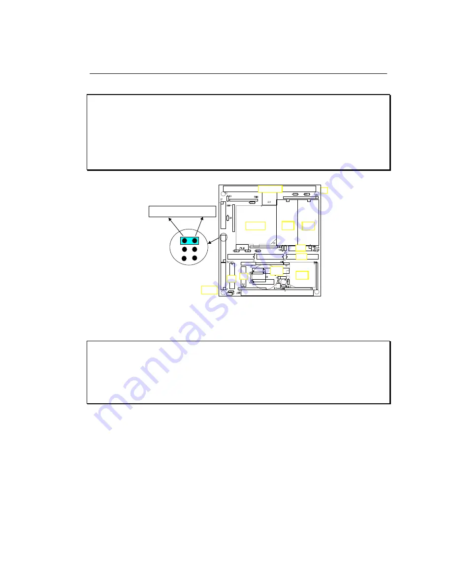
Set the jumper on J10 pins 19 and 20 on the V104 (Figure 1.5).
•
At power-on or reset, if J10 pin 19 (P02) is low, the CPU will run the code that resides in the battery-
backed SRAM.
•
If a jumper is on J10 pins 19-20 at power-on or reset, the V104 will operate in Step Two mode. If the
jumper is off J10 pins 19-20 at power-on or reset, the V104 will operate in Step One mode. The status
of J10 pin 19 (signal P02 of the NEC V25) is only checked at power-on or at reset.
PC/104 Bus
ROM
V25 CPU
RAM
LCD
PPI
SCC
AD
DA
RTC
0, 0
3.5x4.0
pin 20=GND, pin 19=P02
Step 2 jumper
Figure 1.5 Location of Step 2 jumper on the V104
1.4.3
Step 3
STEP 3: Generate the application .BIN or .HEX file, make production ROMs or download your program to
FLASH via ACTF.
•
If you are happy with your Step Two test, you can go back to your PC to generate your application
ROM to replace the DEBUG ROM (TDREM_V25). You need to change DEBUG=1 to DEBUG=0 in
the makefile.
You need to have the DV Kit to complete Step Three.
Please refer to the Tutorial of the Technical Manual of the EV/DV Kit for further details on programming
the V104.
1.5
VE232
The VE232 is an interface board for the V104 that provides reg5V DC power and RS232/485
drivers. It converts TTL signals to and from RS232 signals. You do not need the VE232 if you are using
the V104 installed on another TERN controller such as the P300, PC-Co, MotionC, PowerDrive, or
SensorWatch.
The VE232, shown in Figure 1.6, measures 2.3 x 1.57 inches. A wall transformer (9V, 300 mA) with a
center negative DC plug (Ø=2.0 mm) should be used to power the V104 via the VE232. The VE232


