


73S1209F Data Sheet
DS_1209F_004
Block Guard Time register (
). Other than the protocol checks described above, the firmware is
responsible for all protocol checking and error recovery.
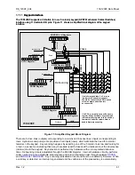
> EGT
< WWT
CHAR 1
CHAR 2
CHAR
N+1
CHAR
N+2
CHAR
N+3
BLOCK1
BLOCK2
> BWT
< CWT
RECEPTION
TRANSMISSION
T = 1 Mode
CHAR 1
CHAR 2
CHAR N
RST
TSTO(7:0)
ATRTO(15:0)
VCC_OK
RLen(7:0)
CHAR 1
CHAR 2
CHAR N
ATR Timing Parameters
IWT(15:0)
BGT(4:0)
TX
T = 0 Mode
IO
EGT
(By seting Last_TXByte and
TX/RXB=0 during CHAR N,
RX mode will start after last
TX byte)
WWT is set by the value in the BWT registers.
Figure 18: Guard, Block, Wait and ATR Time Definitions
1.7.13.4 Bypass
Mode
It is possible to bypass the smart card UART in order for the firmware to support non-T=0/T=1 smart cards.
This is called Bypass mode. In this mode the embedded firmware will communicate directly with the
selected smart card and drive I/O during transmit and read I/O during receive in order to communicate with
the smart card. In this mode, ATR processing is under firmware control. The firmware must sequence the
interface signals as required. Firmware must perform TS processing, parity checking, break generation and
CRC/LRC calculation (if required).
1.7.13.5 Synchronous
Operation
Mode
The 73S1209F supports synchronous operation. When sync mode is selected for either interface, the CLK
signal is generated by the ETU counter. The values in
,
the desired sync CLK rate. There is only one ETU counter and therefore, in sync mode, the interface must
74
Rev.
1.2


